Chip package and manufacturing method thereof

Inactive Publication Date: 2018-01-11
XINTEC INC
View PDF0 Cites 5 Cited by
  • Summary
  • Abstract
  • Description
  • Claims
  • Application Information

AI Technical Summary

Benefits of technology

The present invention relates to a bonding process for semiconductor devices. The invention utilizes a temporary bonding layer to bond a carrier to the semiconductor device. The process includes forming a cavity in the isolation layer, which is a trench, and exposing the side surface of the conductive pad through the cavity. After the redistribution has been formed, the temporary bonding layer and the carrier are removed, resulting in the redistribution layer at least partially protruding from the conductive pad and exposing it. This results in an improved sensing capability of the chip package.

Problems solved by technology

However, after a subsequent dicing process, because the top surface of the chip on which the sensor is disposed and is covered by the dam element, the sensing capability of the chip package is degraded.

Method used


Image

  • Chip package and manufacturing method thereof
  • Chip package and manufacturing method thereof
  • Chip package and manufacturing method thereof

Examples


Embodiment Construction

[0028]Reference will now be made in detail to the present embodiments of the invention, examples of which are illustrated in the accompanying drawings. Wherever possible, the same reference numbers are used in the drawings and the description to refer to the same or like parts.

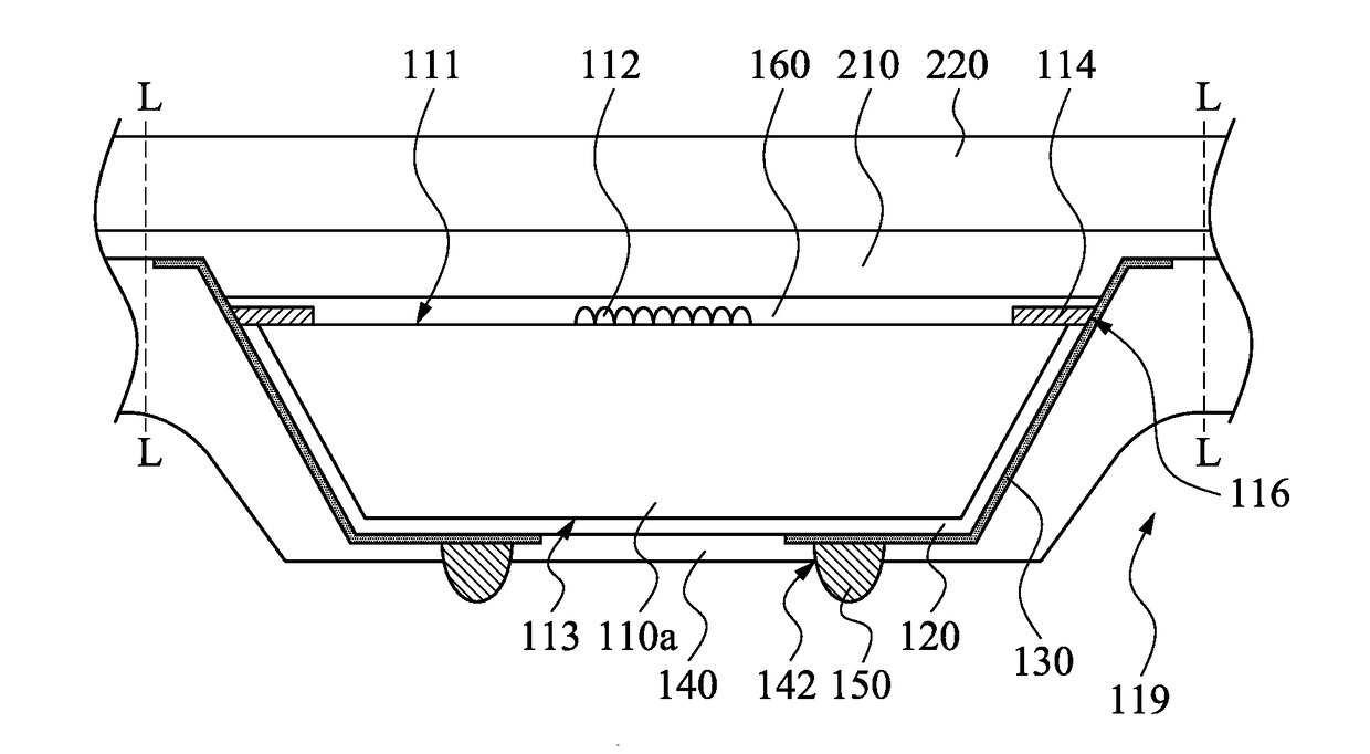
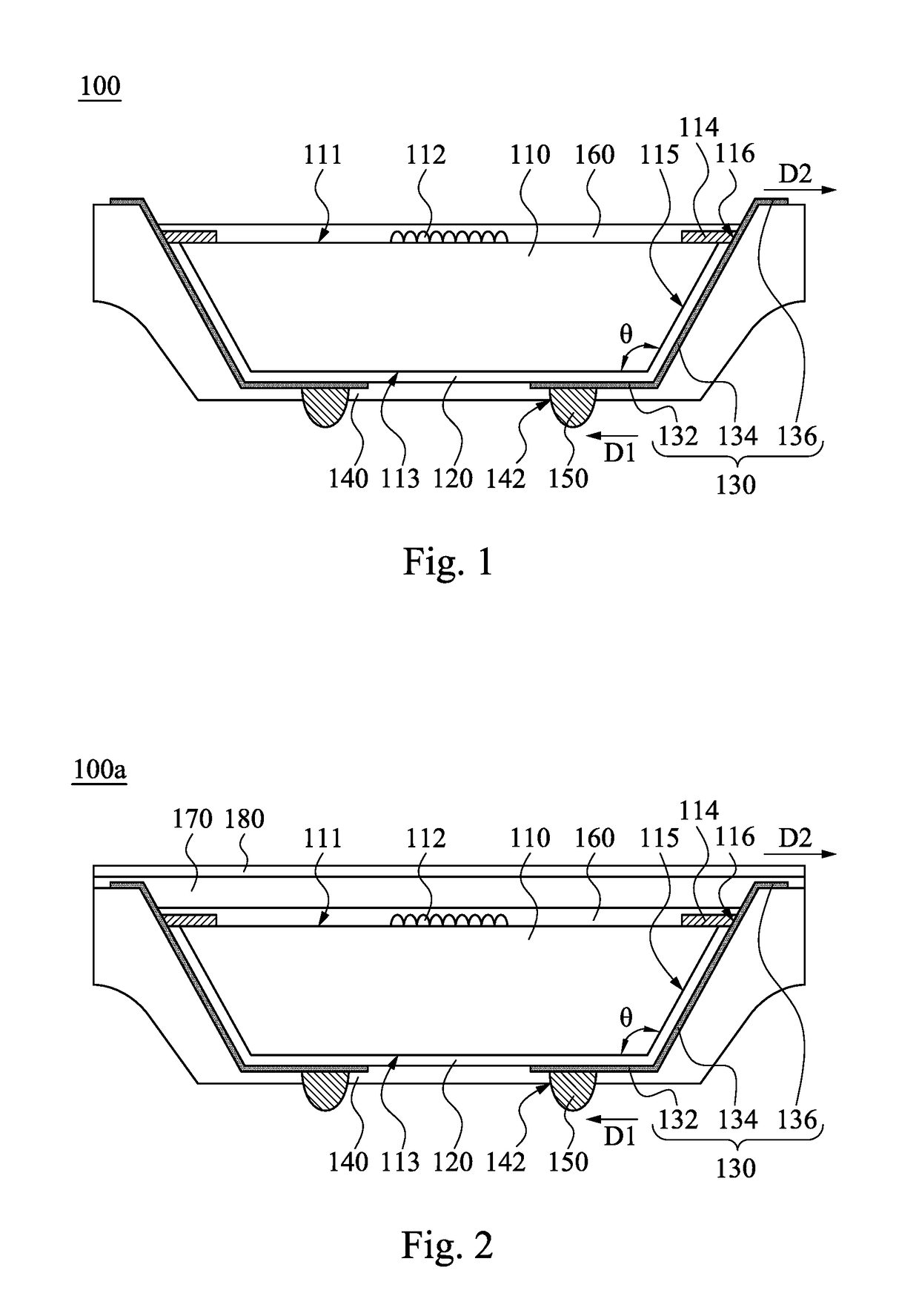
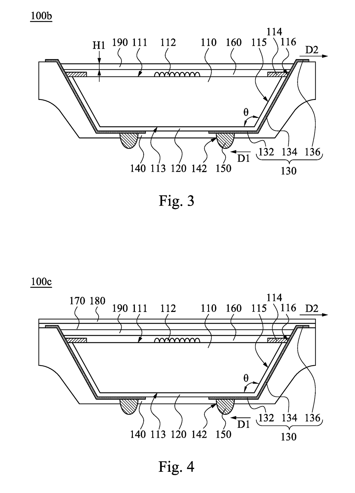
[0029]FIG. 1 is a cross-sectional view of a chip package 100 according to one embodiment of the present invention. As shown in FIG. 1, the chip package 100 includes a chip 110, an isolation layer 120, a redistribution layer 130, and a passivation layer 140. The chip 110 has a sensor 112, at least one conductive pad 114, a top surface 111, a bottom surface 113 that is opposite the top surface 111, and a sidewall 115 adjacent to the top surface 111 and the bottom surface 113. The chip 110 may be made of silicon. The sensor may be an image sensor or fingerprint sensor, such as a CMOS image sensor, but the present invention is not limited in this regard. The sensor 112 is located on the top surface 111, and the co...


PUM


Abstract

A chip package includes a chip, an isolation layer on the bottom surface and the sidewall, a redistribution layer that is on the isolation layer and in electrical contact with a side surface of the conductive pad, and a passivation layer. The chip has a sensor, at least one conductive pad, a top surface, a bottom surface, and a sidewall. The sensor is located on the top surface. The conductive pad is located on an edge of the top surface. The redistribution layer at least partially protrudes from the conductive pad so as to be exposed. The passivation layer is located on the isolation layer and the redistribution layer, such that the redistribution layer not protruding from the conductive pad is between the passivation layer and the isolation layer, and the redistribution layer protruding from the conductive pad is located on the passivation layer.

Description

RELATED APPLICATIONS[0001]This application claims priority to U.S. provisional Application Ser. No. 62 / 360,018, filed Jul. 8, 2016, which is herein incorporated by reference.BACKGROUNDField of Invention[0002]The present invention relates to a chip package and a manufacturing method of the chip package.Description of Related Art[0003]Generally speaking, a chip package used for image sensing or fingerprint sensing may include a chip, a dam element, a redistribution layer (RDL), and a ball grid array (BGA). The redistribution layer may extend to a side surface of the chip from a bottom surface of the chip, such that the redistribution layer on the bottom surface of the chip may be utilized to electrically connect a solder ball of the ball grid array, and the redistribution layer on the side surface of the chip may be utilized to electrically connect the a conductive pad of the chip. As a result, an external electronic device may be electrically connected to an inner line and a sensor o...

Claims


Application Information

Patent Timeline
IPC IPC(8): H01L23/00H01L23/31H01L21/56G06K9/00
CPCH01L24/02H01L24/08H01L23/3171H01L23/3142H01L24/82G06K9/00013H01L2224/02373H01L2224/0236H01L2224/0235H01L2224/02333H01L2224/08221H01L21/56H01L2224/02371H01L2224/0237H01L24/11H01L24/13H01L24/19H01L24/20H01L24/94H01L24/96H01L27/14618H01L2224/02381H01L2224/04105H01L2224/13022H01L2224/13024H01L2224/131H01L2224/73259H01L2224/94H01L2224/96H01L2924/10155H01L2224/03019H01L2224/11002H01L27/1462H01L27/14685H01L2924/00012H01L2924/014H01L2224/0231H01L2224/11H01L2224/19H01L23/3114
Inventor LIN, HSI-CHIENCHEN, JYH-WEIHSIEH, JUN-CHICHEN, YUE-TING
Owner XINTEC INC
Why Eureka
Try Eureka