Semiconductor Module

a technology of semiconductors and modules, applied in the direction of solid-state devices, ac motor stoppers, basic electric elements, etc., can solve the problems of excessive generation of surge voltage across power chips, increased wiring inductance inside packages, etc., and achieve the effect of preventing excessive generation of surge voltag

Active Publication Date: 2018-01-18
MITSUBISHI ELECTRIC CORP
View PDF4 Cites 3 Cited by
  • Summary
  • Abstract
  • Description
  • Claims
  • Application Information

AI Technical Summary

Benefits of technology

[0006]Thus, an emitter wire from the RC-IGBT to an output terminal is drawn with a relatively long loop length, and thereby wiring inductance inside a package may be increased, and a surge voltage generated across a power chip may be excessively generated.
[0007]The present invention has been made to solve the aforementioned problem, and an object of the present invention is to provide a semiconductor module which can prevent excessive generation of a surge voltage generated across a power chip.

Problems solved by technology

Thus, an emitter wire from the RC-IGBT to an output terminal is drawn with a relatively long loop length, and thereby wiring inductance inside a package may be increased, and a surge voltage generated across a power chip may be excessively generated.

Method used


Image

  • Semiconductor Module
  • Semiconductor Module
  • Semiconductor Module

Examples


first embodiment

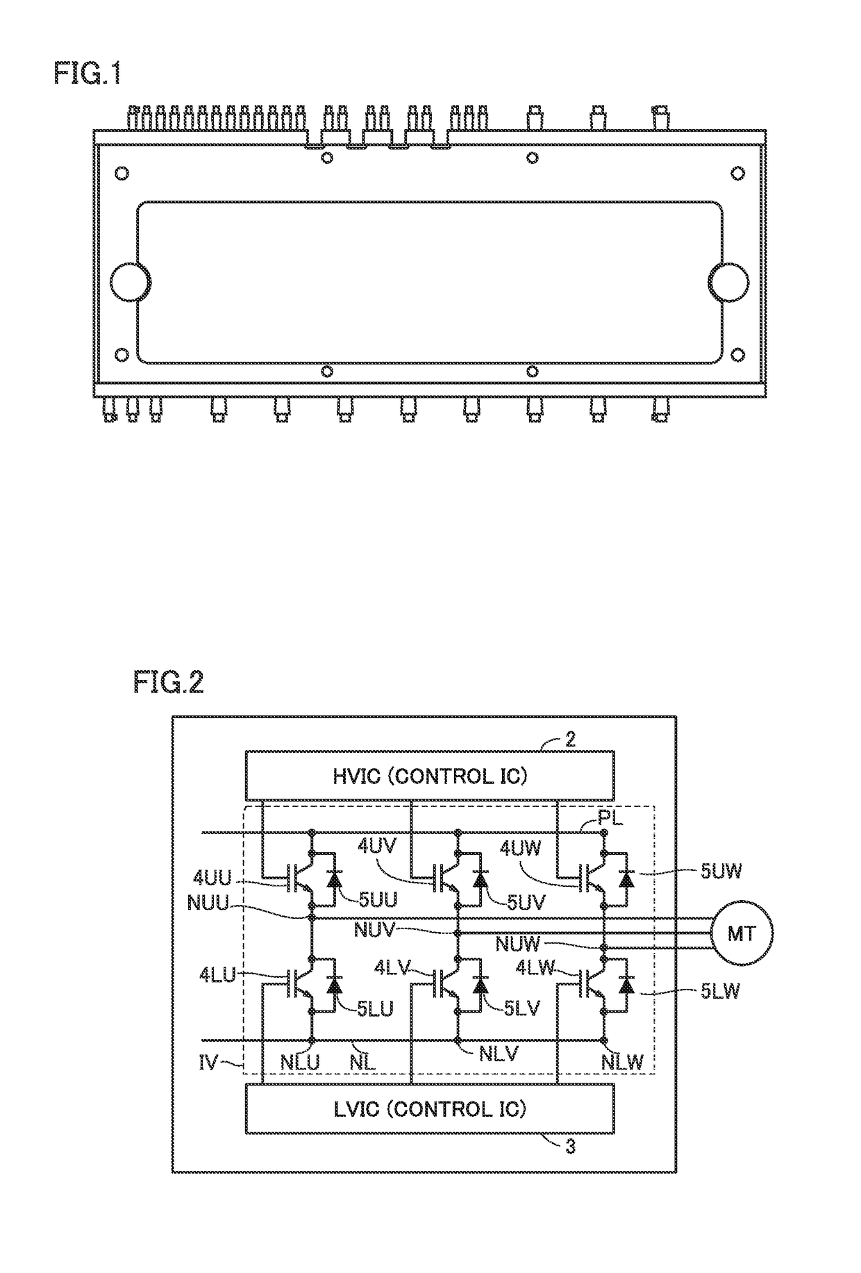
[0023]FIG. 1 is a view showing an outer shape of a transfer mold-type IPM of a first embodiment.

[0024]The transfer mold-type IPM at least includes a control IC and a plurality of power chips. Semiconductor elements in the transfer mold-type IPM are sealed with a mold resin by a transfer mold method.

[0025]FIG. 2 is a view showing components included in the transfer mold-type IPM in the first embodiment.

[0026]The transfer mold-type IPM includes a three-phase inverter IV, a high voltage integrated circuit (HVIC) (control IC) 2, and a low voltage integrated circuit (LVIC) (Control IC) 3.

[0027]The transfer mold-type IPM is connected with a three-phase induction motor MT.

[0028]Three-phase induction motor MT is configured to be driven by a three-phase voltage having different phases. Specifically, in three-phase induction motor MT, a rotating magnetic field is generated around a rotor, which is a conductor, using a three-phase alternating current (AC) having three phases called a U phase, ...

second embodiment

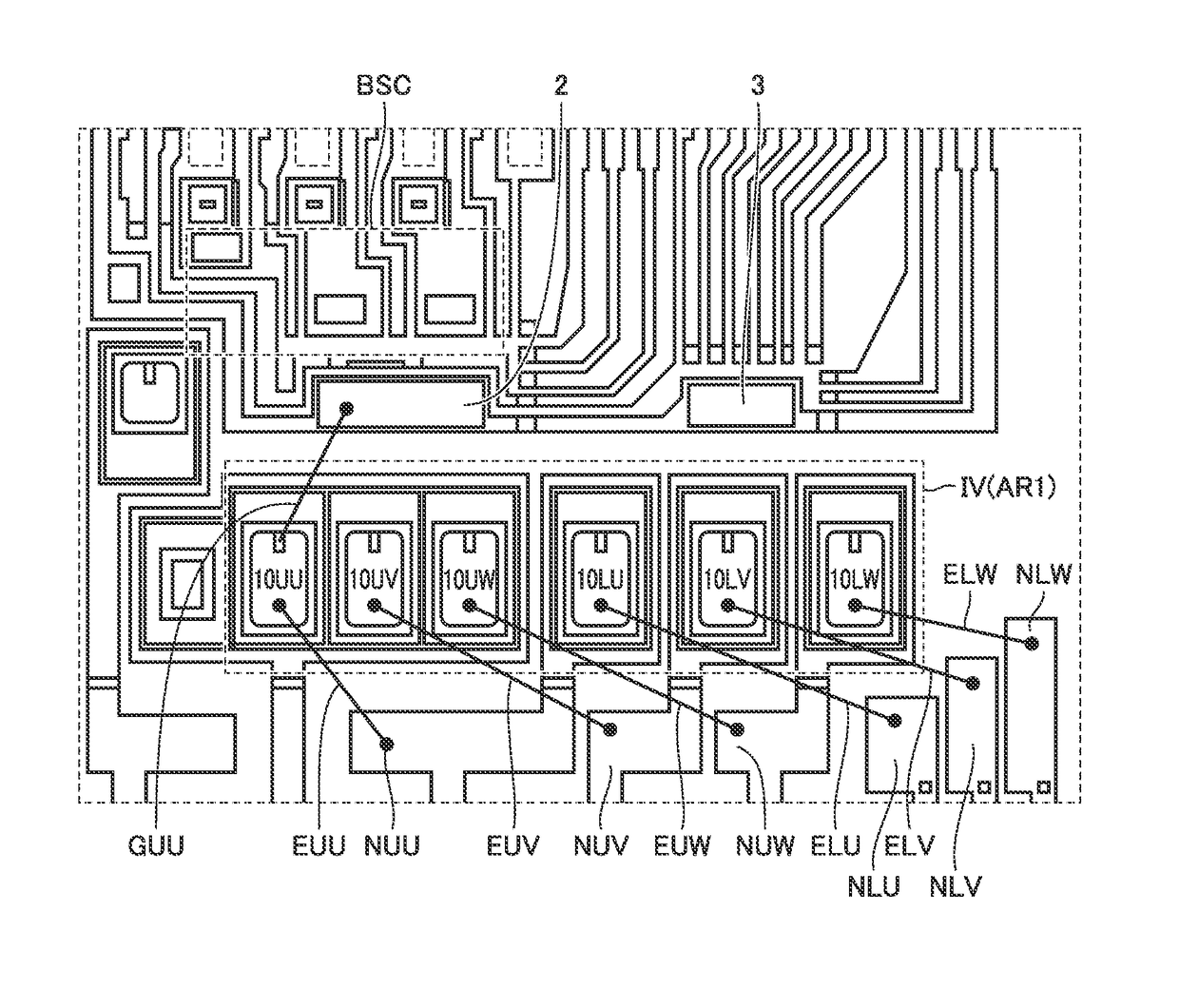
[0052]FIG. 5 is a view showing a layout of a transfer mold-type IPM of a second embodiment.

[0053]Also in the second embodiment. RC-IGBTs 10UU, 10UV, 10UW, 10LU, 10LV, 10LW are arranged in die pad area AR, as in the first embodiment.

[0054]The connection relation between RC-IGBTs 10UU, 10UV, 10UW, 10LU, 10LV, 10LW and HVIC 2, LVIC 3, power terminals NUU, NUV, NUW, NLU, NLV, NLW in the second embodiment is the same as that in the first embodiment.

[0055]In the second embodiment, of two RC-IGBTs for an upper arm and a lower arm of each phase, one is arranged at a position closer to second side L2 than to first side L1 in the Y direction, and the other is arranged at a position closer to first side L1 than to second side L2 in the Y direction.

[0056]Further, six RC-IGBTs are arranged in a staggered pattern along the X direction. That is, of two RC-IGBTs adjacent in the X direction, one is arranged at a position closer to second side L2 than to first side L1 in the Y direction, and the othe...

third embodiment

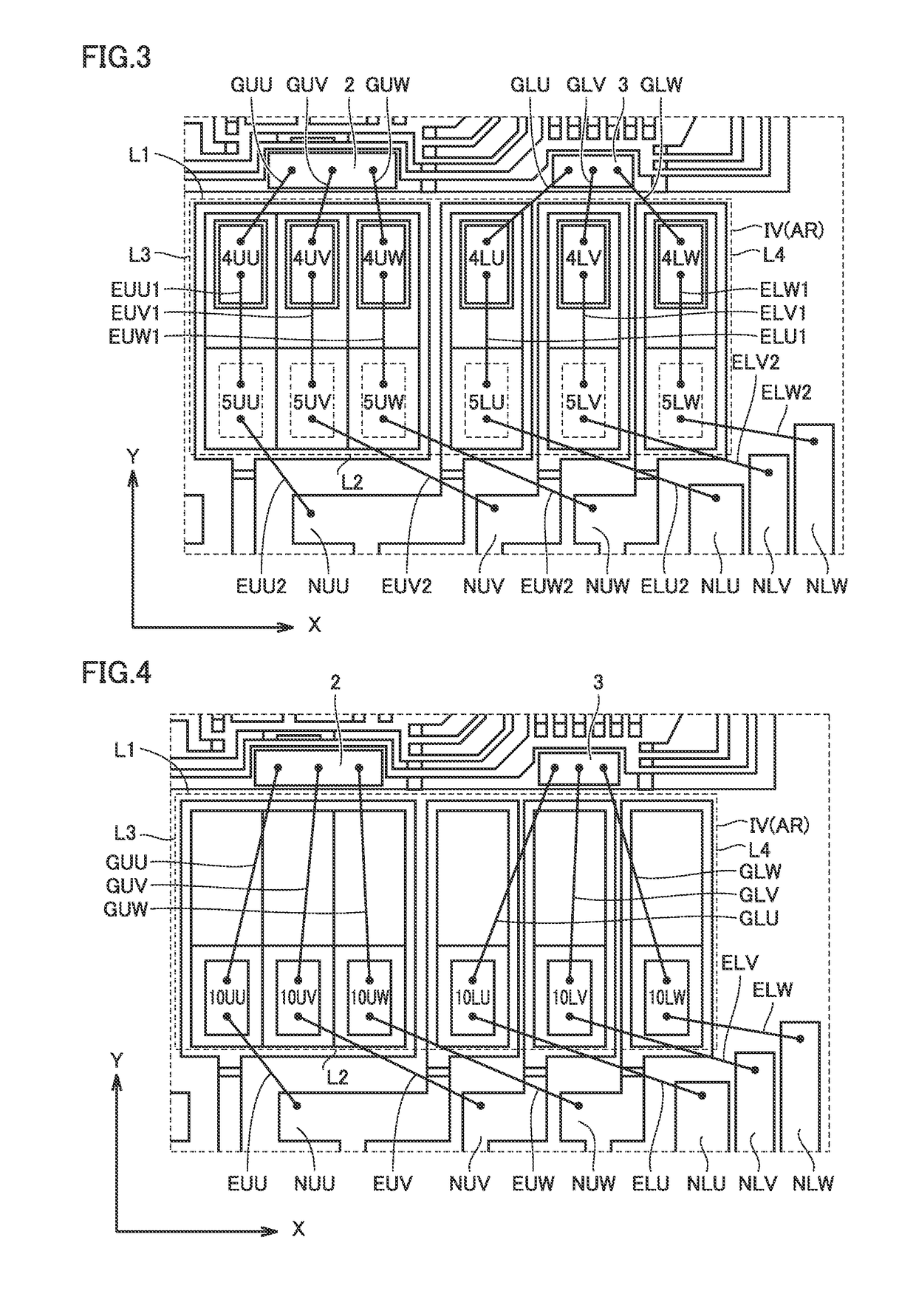
[0062]FIG. 6 is a view showing a layout of a transfer mold-type IPM of a third embodiment.

[0063]Also in the third embodiment, RC-IGBTs 10UU, 10UV, 10UW, 10LU, 10LV, 10LW are arranged in die pad area AR, as in the first embodiment.

[0064]The connection relation between RC-IGBTs 10UU, 10UV, 10UW, 10LU, 10LV, 10LW and HVIC 2, LVIC 3, power terminals NUU, NUV, NUW, NLU, NLV, NLW in the third embodiment is the same as that in the first embodiment.

[0065]In the third embodiment, for each of two of the three phases, of two RC-IGBTs for an upper arm and a lower arm, one is arranged at a position closer to second side L2 than to first side L1 in the Y direction, and the other is arranged at a position closer to first side L1 than to second side L2 in the Y direction. For one of the three phases, both of two RC-IGBTs for an upper arm and a lower arm are each arranged at a substantially central position between first side L1 and second side L2 in the Y direction.

[0066]Die pad area AR is divided ...


PUM


Abstract

A semiconductor module includes a die pad area between positions where a plurality of power terminals are arranged and positions where an HVIC and an LVIC are arranged. A plurality of RC-IGBTs are arranged in the die pad area at positions closer to the plurality of power terminals than to the HVIC and the LVIC.

Description

BACKGROUND OF THE INVENTIONField of the Invention[0001]The present invention relates to a semiconductor module.Description of the Background Art[0002]Conventionally, there has been known a transfer mold-type intelligent power module (IPM) including a reverse conducting insulated gate bipolar transistor (RC-IGBT) and a control IC, the RC-IGBT containing a free wheel diode (hereinafter referred to as FWD) as a power semiconductor element in a chip (see, for example, Japanese Patent Laying-Open No. 2015-135907).[0003]The use of the RC-IGBT eliminates the need for additionally mounting a free wheel diode, which has been necessary when using an ordinary IGBT for an inverter.SUMMARY OF THE INVENTION[0004]However, since it is necessary to unify the outer shape of transfer mold-type IPMs, the transfer mold-type IPM including an RC-IGBT mounted therein should have a pad size equal to that of a transfer mold-type IPM adopting ordinary IGBT and FWD which are not integrated in one chip, in a pl...

Claims


Application Information

Patent Timeline
Patent Type & Authority Applications(United States)
IPC IPC(8): H02P27/06H01L25/07H01L23/538H02M7/5387H02P3/24H01L23/00H01L25/16
CPCH02P27/06H01L25/16H01L24/48H01L23/5386H01L25/072H01L2224/48227H02M7/5387H01L2924/13055H01L2924/1426H01L2924/1425H01L2224/48137H02P3/24H02M1/32H02M7/003H01L2224/0603H01L2924/00014H02P3/22H01L2224/05553H01L2224/04042H01L2924/30107H01L2224/48247H01L2224/32245H01L2224/49112H01L2224/32225H01L2924/19041H01L2924/19043H01L2924/19105H01L2224/24195H01L24/49Y02B70/10H02M1/4291H01L2224/49113H01L2224/45099
Inventor HASEGAWA, MAKISHIRAISHI, TAKUYA
Owner MITSUBISHI ELECTRIC CORP
Why Eureka
Try Eureka