Thin-film transistor array, image display device, and method for manufacturing thin-film transistor array

Active Publication Date: 2018-01-25
TOPPAN PRINTING CO LTD
View PDF7 Cites 0 Cited by
  • Summary
  • Abstract
  • Description
  • Claims
  • Application Information

AI Technical Summary

Problems solved by technology

However, in patterning, yield percentage is lower in printing than in photolithograph

Method used


Image

  • Thin-film transistor array, image display device, and method for manufacturing thin-film transistor array
  • Thin-film transistor array, image display device, and method for manufacturing thin-film transistor array
  • Thin-film transistor array, image display device, and method for manufacturing thin-film transistor array

Examples


first embodiment

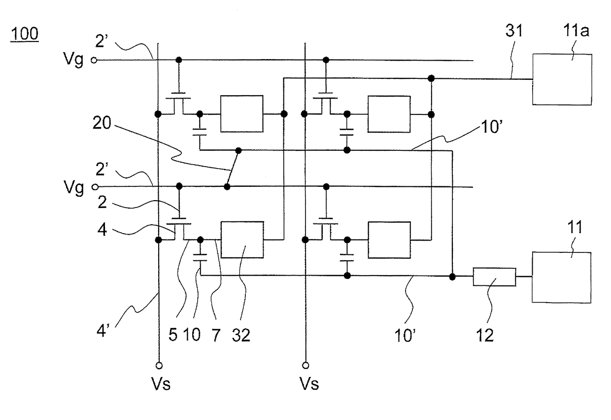
[0038]FIG. 1 illustrates a thin-film transistor array 100 of a first embodiment. The thin-film transistor array 100 includes: an insulating substrate 1; a plurality of gate electrodes 2, a plurality of gate wires 2′ connected to the gate electrodes 2, and a plurality of capacitor electrodes 10, and a plurality of capacitor wires 10′ connected to the capacitor electrodes 10, which are all formed on top of the insulating substrate 1; a gate insulating film 3 which is formed on top of the insulating substrate 1, the gate electrodes 2, the gate wires 2′, the capacitor electrodes 10 and the capacitor electrodes 10; and a plurality of source electrodes 4, a plurality of source wires 4′ connected to the source electrodes 4, a plurality of drain electrodes 5, and a plurality of pixel electrodes 7 connected to the drain electrodes 5, which are all formed on top of the gate insulating film 3. In the thin-film transistor array 100: the pixel electrodes 7 are laid over the respective capacitor ...

second embodiment

[0053]FIG. 4 illustrates a thin-film transistor array 200 of a second embodiment. The thin-film transistor array 200 includes: an insulating substrate 1; a plurality of gate electrodes 2, a plurality of gate wires 2′ connected to the gate electrodes 2, a plurality of capacitor electrodes 10, a plurality of capacitor wires 10′ connected to the capacitor electrodes 10, which are all formed on top of the insulating substrate 1; a gate insulating film 3 which is formed on top of the insulating substrate 1, the gate electrodes 2, the gate wires 2′, the capacitor electrodes 10 and the capacitor electrodes 10; a plurality of source electrodes 4, a plurality of source wires 4′ connected to the source electrodes 4, a plurality of drain electrodes 5, and a plurality of pixel electrodes 7 connected to the drain electrodes 5, which are all formed on top of the gate insulating film 3. In the thin-film transistor array 200: the pixel electrodes 7 are laid over the respective capacitor electrodes ...

example 1

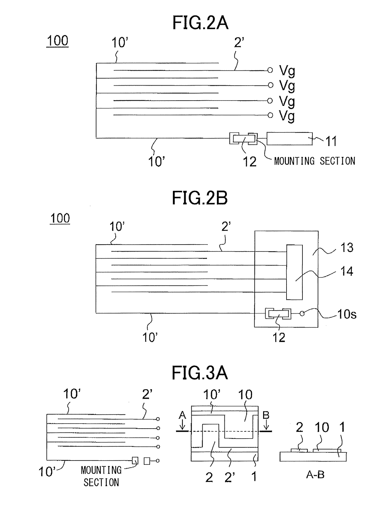
[0077]A specific example will be described. As Example 1, the thin-film transistor array 100 illustrated in FIG. 2A was prepared through the steps illustrated in FIGS. 3A to. 3G. First, using a glass substrate as the insulating substrate 1, Ag ink was off-set printed thereto, followed by baking, thereby forming the gate electrodes 2, the gate wires 2′, the capacitor electrodes 10, and the capacitor wires 10′ (FIG. 3A).

[0078]Then, a polyvinylphenol solution was applied to the resultant object by die coating, followed by baking, thereby forming the gate insulating film 3 (FIG. 3B).

[0079]Then, Ag ink was offset-printed to the resultant object, followed by baking, thereby forming the source electrodes 4, the source wires 4′, the drain electrodes 5, and the pixel electrodes 7 (FIG. 3C). Then, a polythiophene type organic semiconductor solution was printed to the resultant object by flexographic printing, followed by baking, thereby forming the semiconductor layer 6 (FIG. 3D). Then, a flu...


PUM


Abstract

A thin-film transistor array including an insulating substrate, a gate insulating film sandwiched between a first structure and a second structure, the first structure including a gate electrode, a gate wire connected to the gate electrode, a capacitor electrode, and a capacitor wire connected to the capacitor electrode, and the second structure including a source electrode, a source wire connected to the source electrode, a drain electrode, and a pixel electrode connected to the drain electrode, a resistor inserted between parts of the capacitor wire, and a semiconductor layer formed between the source electrode and the drain electrode. The pixel electrode is positioned over the capacitor electrode with the gate insulating film positioned therebetween and has a storage capacitance, and the source electrode and the drain electrode are positioned over the gate electrode with the gate insulating film positioned therebetween.

Description

CROSS-REFERENCE TO RELATED APPLICATIONS[0001]The present application is a continuation of International Application No. PCT / JP2016 / 001570, filed Mar. 17, 2016, which is based upon and claims the benefits of priority to Japanese Application No. 2015-054712, filed Mar. 18, 2015. The entire contents of these applications are incorporated herein by reference.BACKGROUND OF THE INVENTIONField of the Invention[0002]The present invention relates to a thin-film transistor array, an image display device, and a method for manufacturing a thin-film transistor array.Discussion of the Background[0003]With the development of thin-film transistors, liquid-crystal display devices or electrophoretic display devices that use thin-film transistors are being developed. Typically, photolithography has been used when patterning thin-film transistor array electrodes.[0004]In recent years, printed thin-film transistor arrays have attracted attention as less expensive thin-film transistor arrays, or as thin-...

Claims


Application Information

Patent Timeline
IPC IPC(8): G02F1/1343H01L29/786H01L21/822G02F1/1362
CPCG02F1/1343G02F1/1362H01L29/786H01L21/822G09F9/35G03F7/00G09F9/30H01L27/04G02F1/136204H01L27/1255H01L27/1292H01L27/1222
Inventor ISHIZAKI, MAMORU
Owner TOPPAN PRINTING CO LTD
Why Eureka
Try Eureka