
Microelectromechanical device, a microelectromechanical system, and a method of manufacturing a microelectromechanical device

Active Publication Date: 2018-02-01
INFINEON TECH AG
View PDF2 Cites 8 Cited by
  • Summary
  • Abstract
  • Description
  • Claims
  • Application Information

AI Technical Summary

Benefits of technology

The invention describes a device that includes a diaphragm and a special electrode structure. The electrodes are arranged in a way that reduces noise and improves resolution at low frequencies. This makes it easier to detect and measure small amounts of electrical activity. The device can be used in a variety of applications such as medical sensors or biological research. The technical effect of this invention is improved precision and accuracy in measuring small quantities of electrical activity.

Problems solved by technology

The signal to noise ratio in such arrangements may be limited by air friction in the perforated back plate that causes noise.
In comparison, MEMS with a comb electrode structure may have significantly reduced noise due to the comb electrode arrangement, however, comb electrode structures have large ventilation areas (for example, gaps, through which incident sounds (e.g., a pressure wave) may pass without significantly affecting the diaphragm), which reduce resolution of low frequency sound.
This solution is limited by dimensional feasibility allowed by various fabrication methods.

Method used


Image

  • Microelectromechanical device, a microelectromechanical system, and a method of manufacturing a microelectromechanical device
  • Microelectromechanical device, a microelectromechanical system, and a method of manufacturing a microelectromechanical device
  • Microelectromechanical device, a microelectromechanical system, and a method of manufacturing a microelectromechanical device

Examples


example 3

[0089 may include the microelectromechanical device of any one of Examples 1 and 2, wherein the substrate is formed from a semiconductor.

[0090]Example 4 may include the microelectromechanical device of Example 3, wherein the semiconductor is silicon.

[0091]Example 5 may include the microelectromechanical device of any one of Examples 1-3, wherein the diaphragm is formed from an electrically conductive material.

example 6

[0092 may include the microelectromechanical device of Example 5, wherein the electrically conductive material is a metal.

example 7

[0093 may include the microelectromechanical device of Example 6, wherein the electrically conductive material is a semiconductor.

[0094]Example 8 may include the microelectromechanical device of Example 7, wherein the semiconductor is silicon.

[0095]Example 9 may include the microelectromechanical device of Example 8, wherein the silicon is a polycrystalline silicon.


PUM

PropertyMeasurementUnit
Distanceaaaaaaaaaa

Abstract

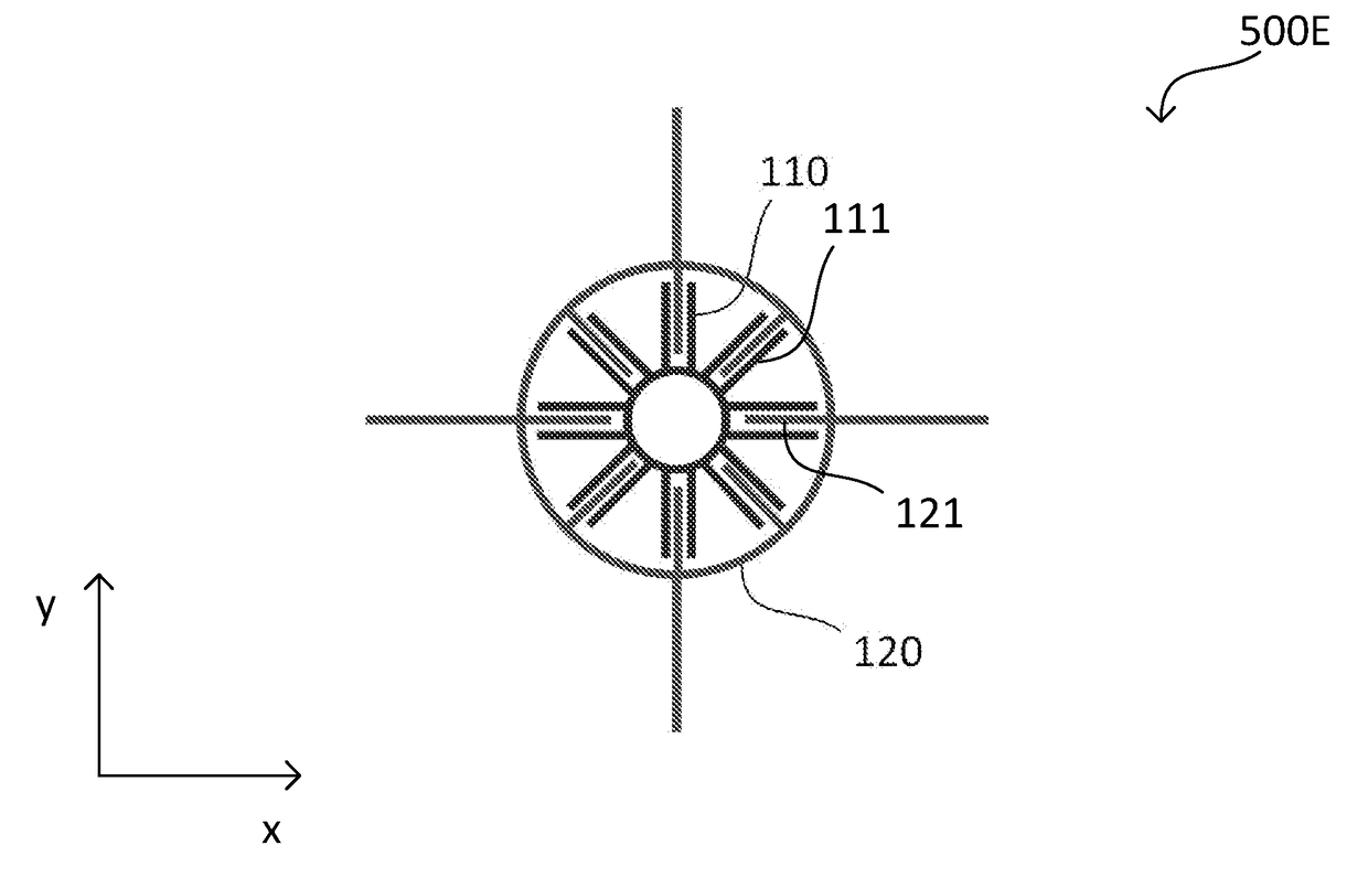
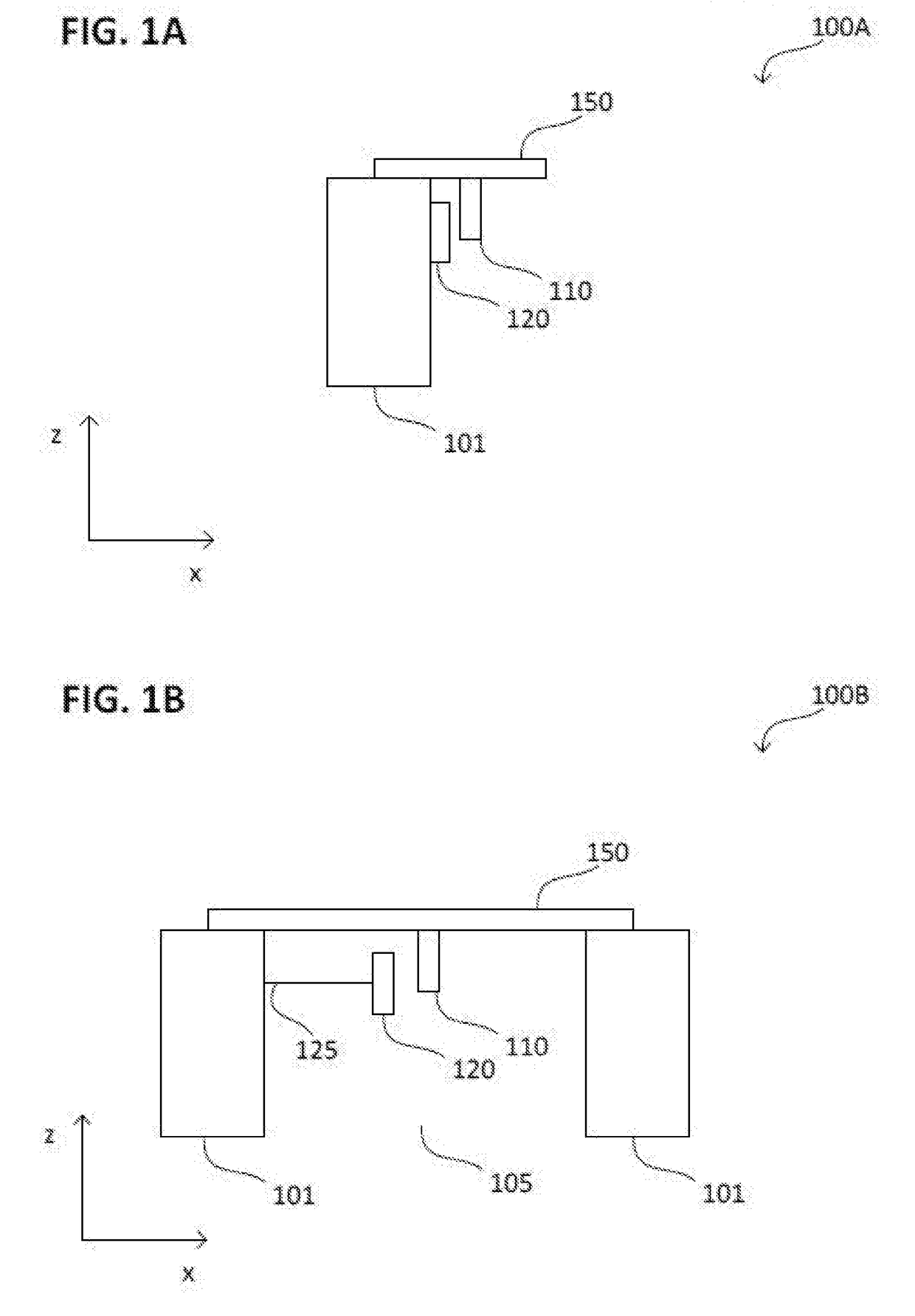
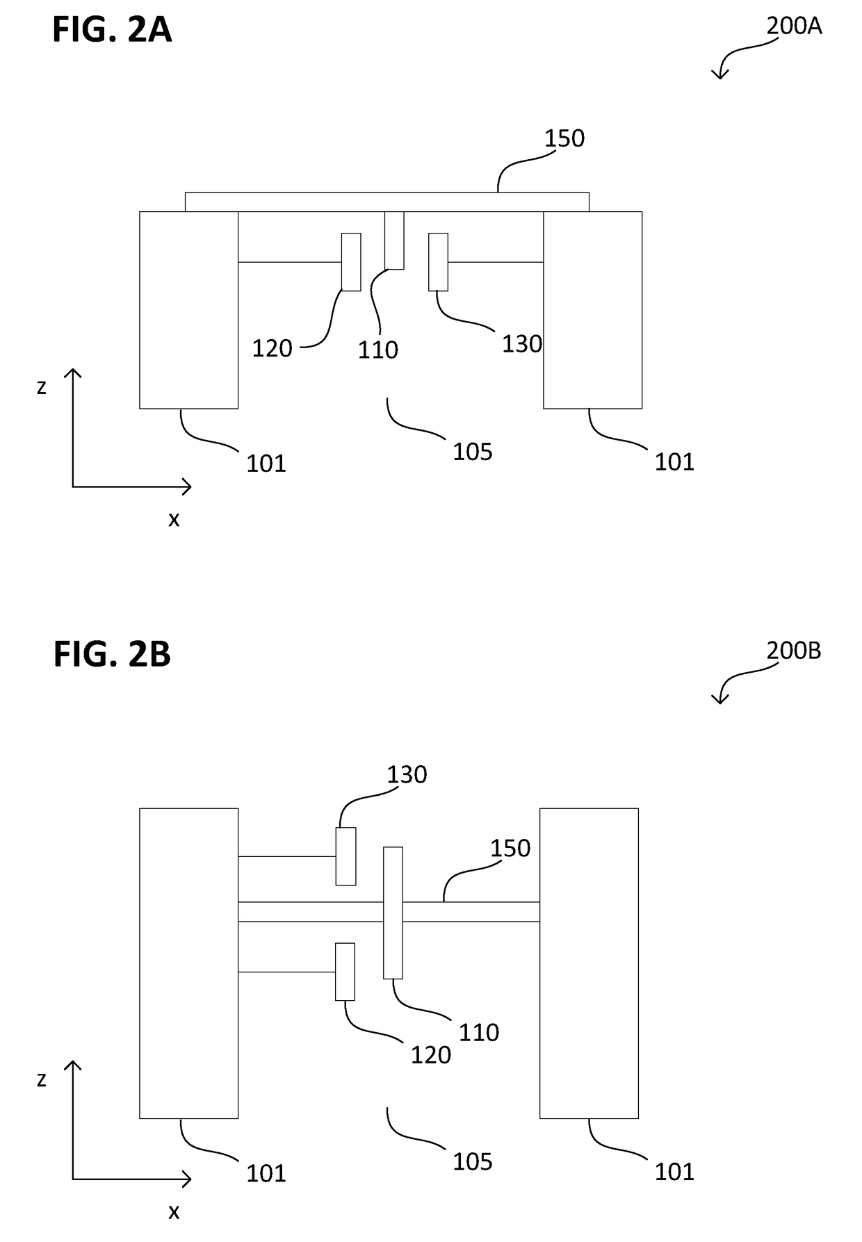
A microelectromechanical device, a microelectromechanical system, and a method of manufacturing a microelectromechanical device, wherein the microelectromechanical device may include: a substrate; a diaphragm mounted to the substrate; a first electrode mounted to the diaphragm; a second electrode mounted to the substrate; wherein the first electrode is laterally adjacent to the second electrode; and wherein the diaphragm is arranged over a gap between the first electrode and the second electrode.

Description

CROSS-REFERENCE TO RELATED APPLICATION[0001]This application claims priority to German Patent Application Serial No. 10 2016 114 047.3, which was filed Jul. 29, 2016, and is incorporated herein by reference in its entirety.TECHNICAL FIELD[0002]Various embodiments relate generally to a microelectromechanical device, a microelectromechanical system, and a method of manufacturing a microelectromechanical device.BACKGROUND[0003]Silicon microelectromechanical systems (MEMS), for example, a MEMS microphone, may have a pressure sensitive diaphragm and a perforated back plate to provide an electrostatic read out. The signal to noise ratio in such arrangements may be limited by air friction in the perforated back plate that causes noise. In comparison, MEMS with a comb electrode structure may have significantly reduced noise due to the comb electrode arrangement, however, comb electrode structures have large ventilation areas (for example, gaps, through which incident sounds (e.g., a pressur...

Claims


Application Information

Patent Timeline
IPC IPC(8): B81B7/00B81C1/00B81B3/00
CPCB81B7/0061B81B3/0021B81B2203/0127B81C1/00166B81B2203/04B81C1/00158B81B3/0067B81B7/0009B81B7/02B81C3/001B81B2201/0257B81B2201/033
Inventor DEHE, ALFONSHERRMANN, MATTHIAS FRIEDRICHMANZ, JOHANNES
Owner INFINEON TECH AG
Learn More