Camera Module, Molded Circuit Board Assembly, Molded Photosensitive Assembly and Manufacturing Method Thereof

a technology of camera modules and molded circuit boards, which is applied in the direction of sustainable manufacturing/processing, instruments, television systems, etc., can solve the problems of not being able to produce the ideal structure of the camera module by conventional methods, not being able to achieve very good and practical implements that have not been put into actual production, and only staying in packaging technology, etc., to achieve smooth pulling out, reduce friction with the molded base, and reduce the effect of light window forming blocks

Active Publication Date: 2018-02-01
NINGBO SUNNY OPOTECH CO LTD
View PDF9 Cites 10 Cited by
  • Summary
  • Abstract
  • Description
  • Claims
  • Application Information

AI Technical Summary

Benefits of technology

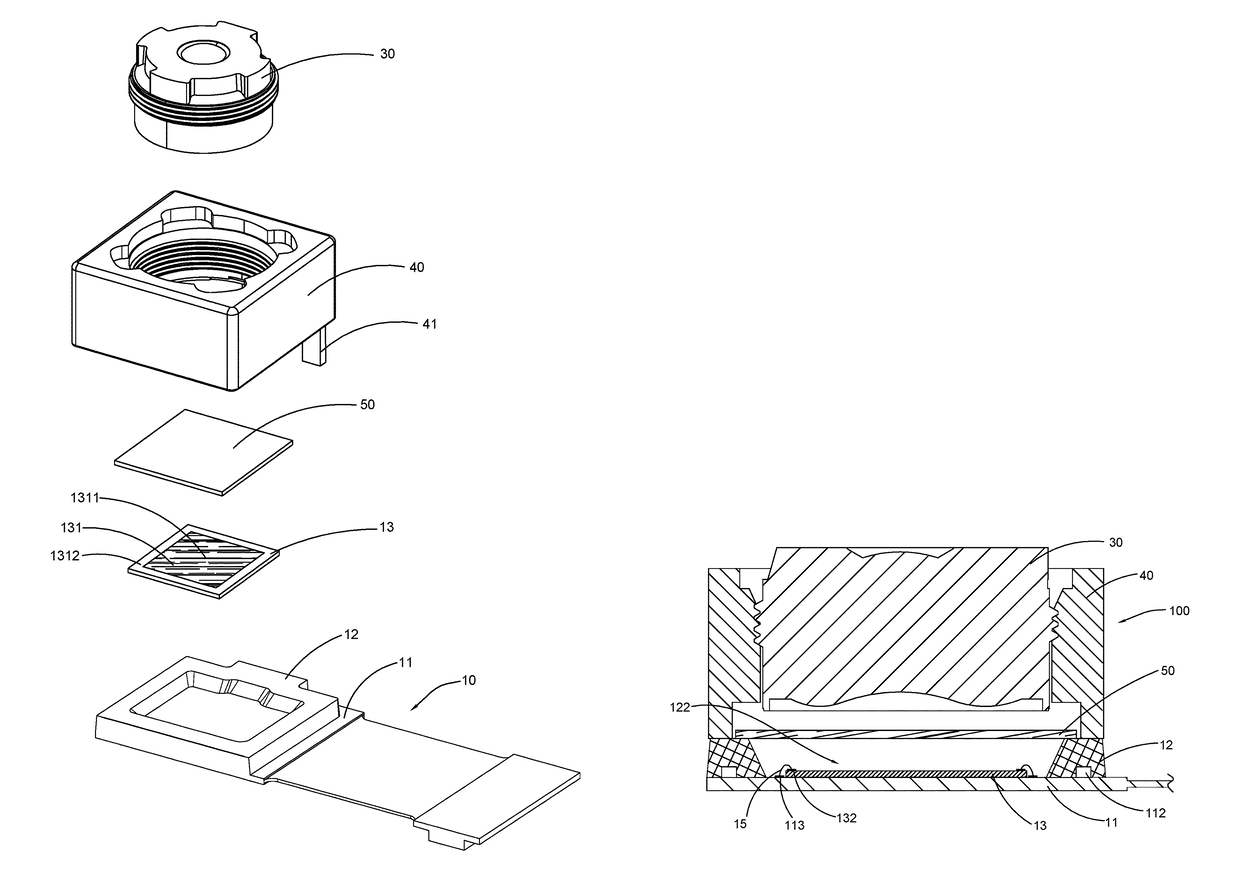
[0012]Another advantage of the invention is to provide a camera module and its molded circuit board assembly and manufacturing method thereof, wherein the molded circuit board assembly comprises a circuit board and a molded base integrally formed on the circuit board, wherein the molded base forms a light window, which is not a prismatic column shape of the prior art, so that in a manufacturing process, the damage to the molded base by a light window forming block of a molding mould is reduced, and it is convenient to remove the light window forming block.
[0013]Another advantage of the invention is to provide a camera module and its molded circuit board assembly and manufacturing method thereof, wherein at least one portion of the molded base integrally extended from the circuit board and an optical axis direction form a first inclination angle which is an acute angle and is benefit for demoulding of the molded base. In which, after the molded base is formed by the molding process, the light window forming block is able to be smoothly pulled out to reduce friction with the molded base so that said molded base is remained unchanged to reduce the influence of the removal of the light window forming block.
[0014]Another advantage of the invention is to provide a camera module and its molded circuit board assembly and manufacturing method thereof, wherein at least one portion of the inner side surface of the molded base integrally extended from the top surface of the circuit board and the optical axis form an angle which is defined as a first inclination angle, so that the light incident on the inner side surface is less likely to reach the photosensitive element, and the influence of the stray light on the image quality is reduced.
[0015]Another advantage of the invention is to provide a camera module and its molded circuit board assembly and manufacturing method thereof, wherein at least one outer side surface of the molded base and the optical axis form an angle which is an acute angle and is defined as a second inclination angle, wherein when the molded base is manufactured by the molding mould and the dividing blocks of the molding mould are detached at the outside of the molded base, the friction between the dividing blocks of the molding mould and the outer side surface of the molded base is remained unchanged such that the dividing blocks of the molding mould are easy to demould and remove.
[0016]Another advantage of the invention is to provide a camera module and its molded circuit board assembly and manufacturing method thereof, wherein the inner side of the molded base successively has a first portion inner side surface inclined from the circuit board, a second portion inner side surface extending from the first portion inner side surface, and a third portion inner side surface aslant extending from the second portion inner side surface, wherein the third portion inner side surface and the optical axis form an angle which is an acute angle and is defined as a third inclination angle, so that when the light window forming block of the molded base is removed, the friction between the base portion of the light window forming block and the inner side of the top end of the molded base is reduced, and thus the second portion inner side surface of the molded base is remained unchanged such that the dividing blocks of the molding mould are easy to demould and remove.
[0017]Another advantage of the invention is to provide a camera module and its molded circuit board assembly and manufacturing method thereof, wherein the first inclination angle is in a predetermined range to facilitate pulling out the molded base without damaging the molded base.

Problems solved by technology

However, in a period of time, this packaging technology only stays in the theoretical or manual experimental stages, and fails to achieve very good and practical implement that has not been put into actual production for quantitative production.
It is understandable that components of the camera module are manufactured in a relatively small size, so that the ideal structure of the camera module cannot be produced by conventional methods.
Theoretically speaking, this conceptual structure does not have much substantial defects, but it does fail to take various mass production factors into account.
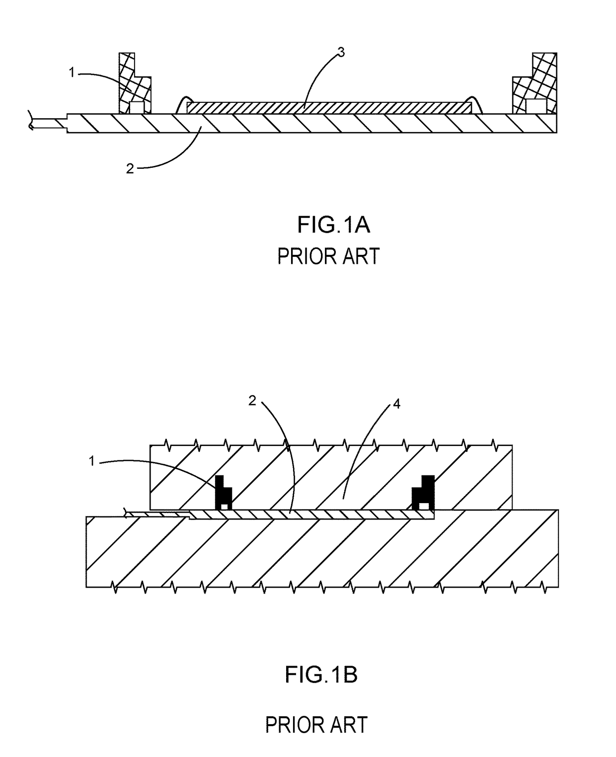
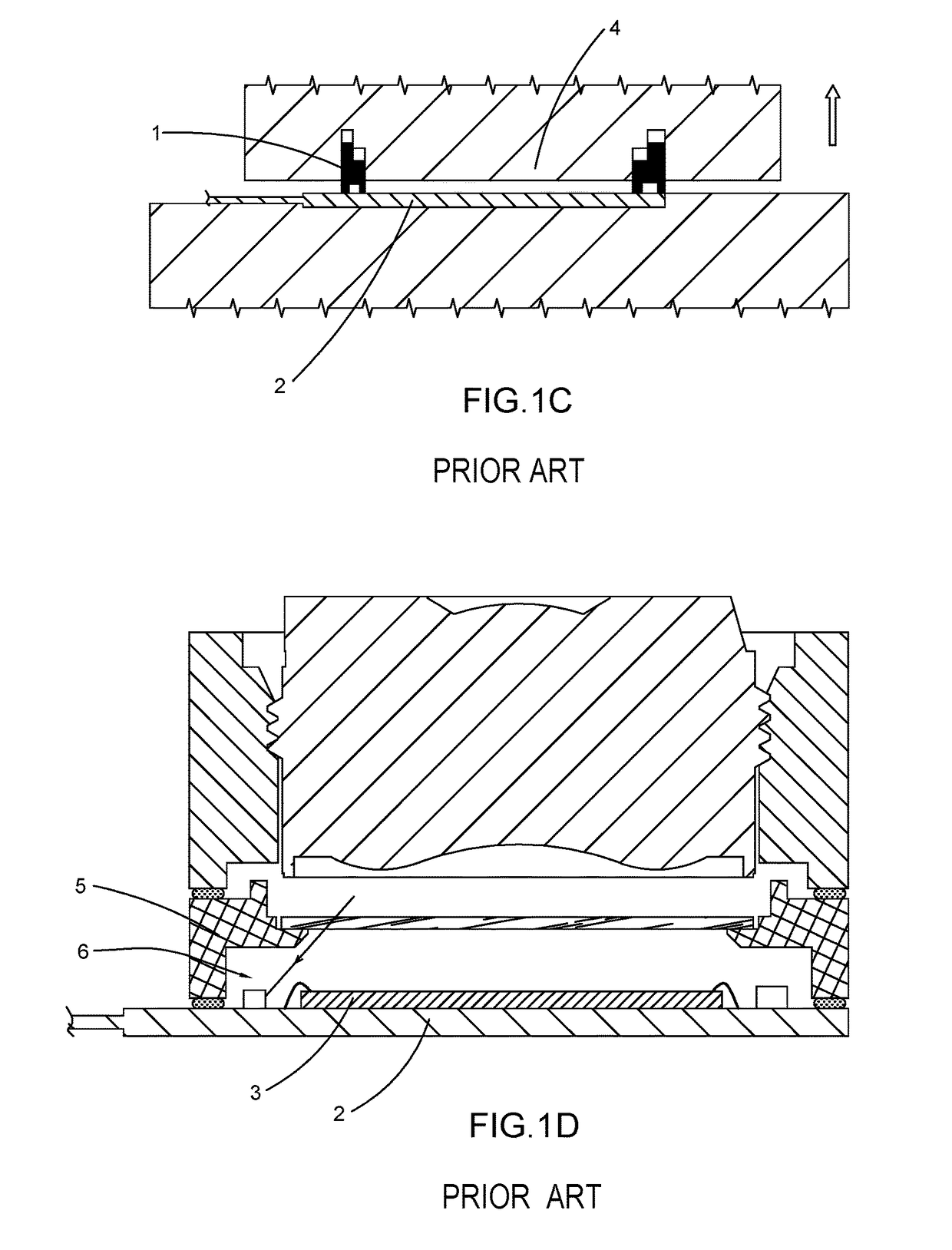
Therefore, the vertical prismatic column shaped through-hole structure is feasible in theory but is not suitable for mass productions in practice.
Accordingly, in the aspect of the optical imaging quality, such rectangular shaped through-hole configuration formed in encapsulation portion 1 is not suitable for utility application.
However, the structure of the conventional encapsulation portion 1 apparently failed to encounter all such factors under consideration.

Method used


Image

  • Camera Module, Molded Circuit Board Assembly, Molded Photosensitive Assembly and Manufacturing Method Thereof
  • Camera Module, Molded Circuit Board Assembly, Molded Photosensitive Assembly and Manufacturing Method Thereof
  • Camera Module, Molded Circuit Board Assembly, Molded Photosensitive Assembly and Manufacturing Method Thereof

Examples


first embodiment

[0168]It is understandable that, in comparison with the manufacturing process of the separated molded circuit board assembly 10 in the above first embodiment of the present invention, in the joint board array operation, two adjacent base forming guide grooves 215 forming two molded bases 12 are jointed together while the light window forming blocks 214 are spaced with each other, so that the molding material 14 eventually forms the integral piece of molded base array 1200 with an overall configuration.

[0169]In the step of manufacturing the separated molded circuit board assembly 10, the integral piece of molded circuit board assembly array 1000 is cut into a plurality of molded circuit board assemblies 10 to manufacture a plurality of camera modules respectively. Alternatively, two or more molded circuit board assemblies 10 which are combined with each other from the integral piece of molded circuit board assembly array 1000 can be separated and manufactured by cutting so as to manu...

third embodiment

[0223]It is understandable that, a molding process of the circuit board 11′ is illustrated, wherein, in the application of the manufacturing equipment 200′, a plurality of separated circuit boards 11′ can be molded at the same time. Alternatively, a joint board array operation mentioned in the following embodiment is also adapted.

[0224]Referring to FIG. 36A to FIG. 36C of the drawings, a manufacturing process of the molded photosensitive assembly 10′ of the camera module 100′ according to the preferred embodiment of the present invention is illustrated. As shown in FIG. 36A of the drawings, the molding mould 210′ is in the closed-mould position, the circuit board 11′ which is about to be molded and the solid molding material 14′ are placed in position therein. The solid molding material 14′ is heated and melted into a liquid state or into a semi-solid state, which is pressured to fill into the base forming guide groove 215′ until reaching around the light window forming block 214′....


PUM

PropertyMeasurementUnit
inclination angleaaaaaaaaaa

Abstract

A camera module, a molded circuit board assembly, a molded photosensitive assembly and manufacturing method thereof are disclosed. The camera module includes a molded base which is integrally formed with a circuit board through a molding process, wherein a photosensitive element may be electrically connected on the circuit board and at least a portion of a non-photosensitive area portion of the photosensitive element is also connected by the molded base through the molding process. A light window is formed in a central portion of the molded base to provide a light path for the photosensitive element, wherein a cross section of the light window is configured to have a trapezoidal or multi-step trapezoidal shape which has a size increasing from bottom to top to facilitate demoulding and avoiding stray lights.

Description

CROSS REFERENCE OF RELATED APPLICATION[0001]This is Continuation application that claims the benefit of priority under 35U.S.C.§120 to a non-provisional application, application Ser. No. 15 / 439,909, filed Feb. 22, 2017, that claims priority to China application number CN201610622330.3, filed Aug. 1, 2016, China application number CN201620826033.6, filing date Aug. 1, 2016, China application number CN201610626667.1, filed Aug. 1, 2016, and China application number CN201620826035.5, filed Aug. 1, 2016, which are incorporated herewith by reference in their entities.NOTICE OF COPYRIGHT[0002]A portion of the disclosure of this patent document contains material which is subject to copyright protection. The copyright owner has no objection to any reproduction by anyone of the patent disclosure, as it appears in the United States Patent and Trademark Office patent files or records, but otherwise reserves all copyright rights whatsoever.BACKGROUND OF THE PRESENT INVENTIONField of Invention[0...

Claims


Application Information

Patent Timeline
Patent Type & Authority Applications(United States)
IPC IPC(8): H04N5/225B29C43/18B29C43/52B29C43/36G02B7/10G02B7/02B29L31/00
CPCB29L2031/764B29C43/52B29C43/36B29C43/18H04N5/2257H04N5/2253G02B7/10G02B7/022H04N5/2254B29L2031/3437B29C45/14655B29C45/40B29C33/44B29C45/0025G02B19/0014G02B19/0076B29C70/72B29L2031/3425B29C45/14336H05K1/181H05K3/284H05K2201/10121H05K2203/1316H05K2203/1327H01L27/14618H01L27/14625Y02P70/50H04N23/54H04N23/57H04N23/55H05K1/0274H05K1/185B29C45/14467B29C70/88G02B13/0085B29C45/14819B29D11/00807B29K2101/12B29K2995/0003B29K2995/0018H05K2203/0195
Inventor WANG, MINGZHUCHEN, ZHENYUGUO, NANTANAKA, TAKEHIKOZHAO, BOJIEDENG, ZILONG
Owner NINGBO SUNNY OPOTECH CO LTD
Why Eureka
Try Eureka