

Blue-phase liquid crystal panels and manufacturing methods of liquid crystal panels thereof
- Summary
- Abstract
- Description
- Claims
- Application Information
AI Technical Summary
Benefits of technology
Problems solved by technology
Method used
Image

Examples
first embodiment
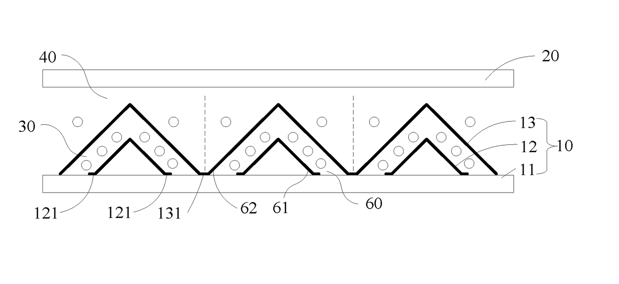
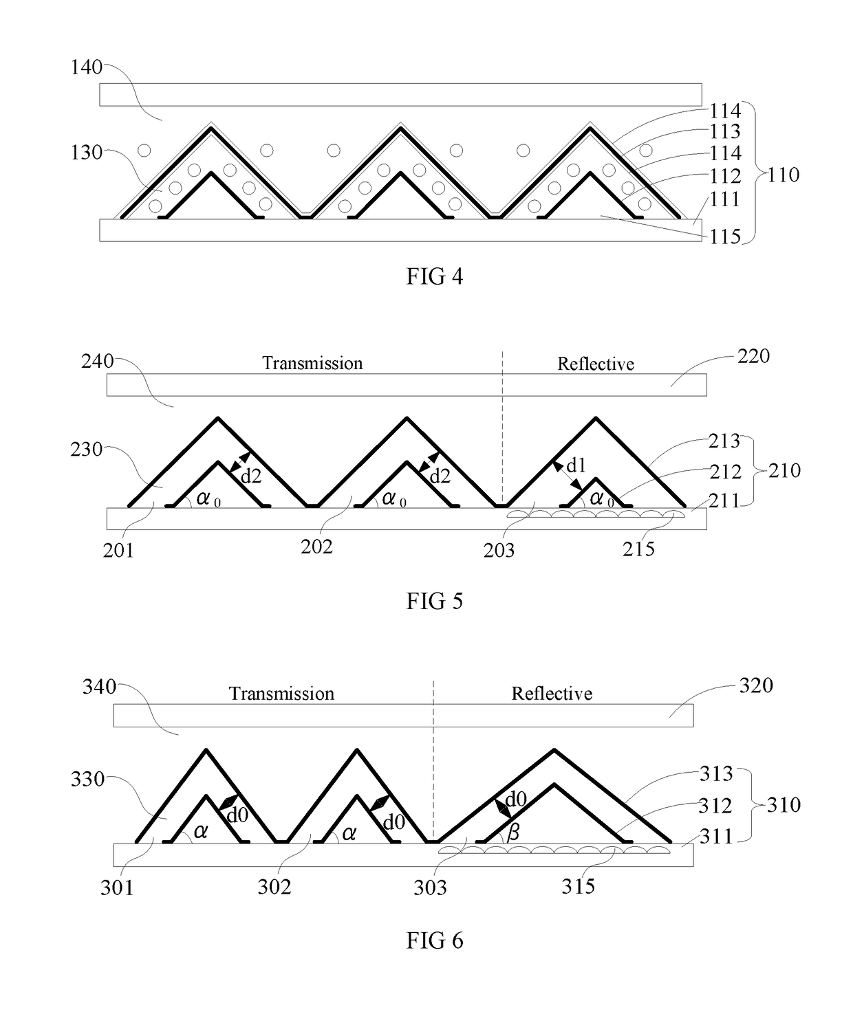
[0052]With respect to ripple unit 203 corresponding to the reflective display area, a first gap between the first electrode layer 212 and the second electrode layer 213 is d1, and a second gap between the first electrode layer 212 and the second electrode layer 213 within the ripple units 201, 202 corresponding to the transmission display area is d2. In addition, the driving voltages of the ripple units 201, 202, and 203 are the same, and the inclined angle of the ripple are α0. The first substrate 211 may further include an insulation layer (not shown) on the top surface and / or the down surface of the second electrode layer 213. The blue-phase liquid crystals are not shown, but it can be understood that the blue-phase liquid crystals are distributed within the first space 230 and the second space 240 by referencing the
[0053]The relationship between d1 and d2 may be adjusted such that the phase delay of the light beams passing through the ripple units respectively within the transmi...
second embodiment
[0068]The relationship between d3 and d4 may be adjusted such that the phase delay of the light beams passing through the ripple units respectively within the transmission and reflective display area may be the same. The calculations and testing of the relationship between d3 and d4 may be understood by referring to the second embodiment, and thus are omitted hereinafter.
[0069]Compared to the second embodiment, the transmission display area and the reflective display area are combined within one ripple unit so as to realize transflective display panel.
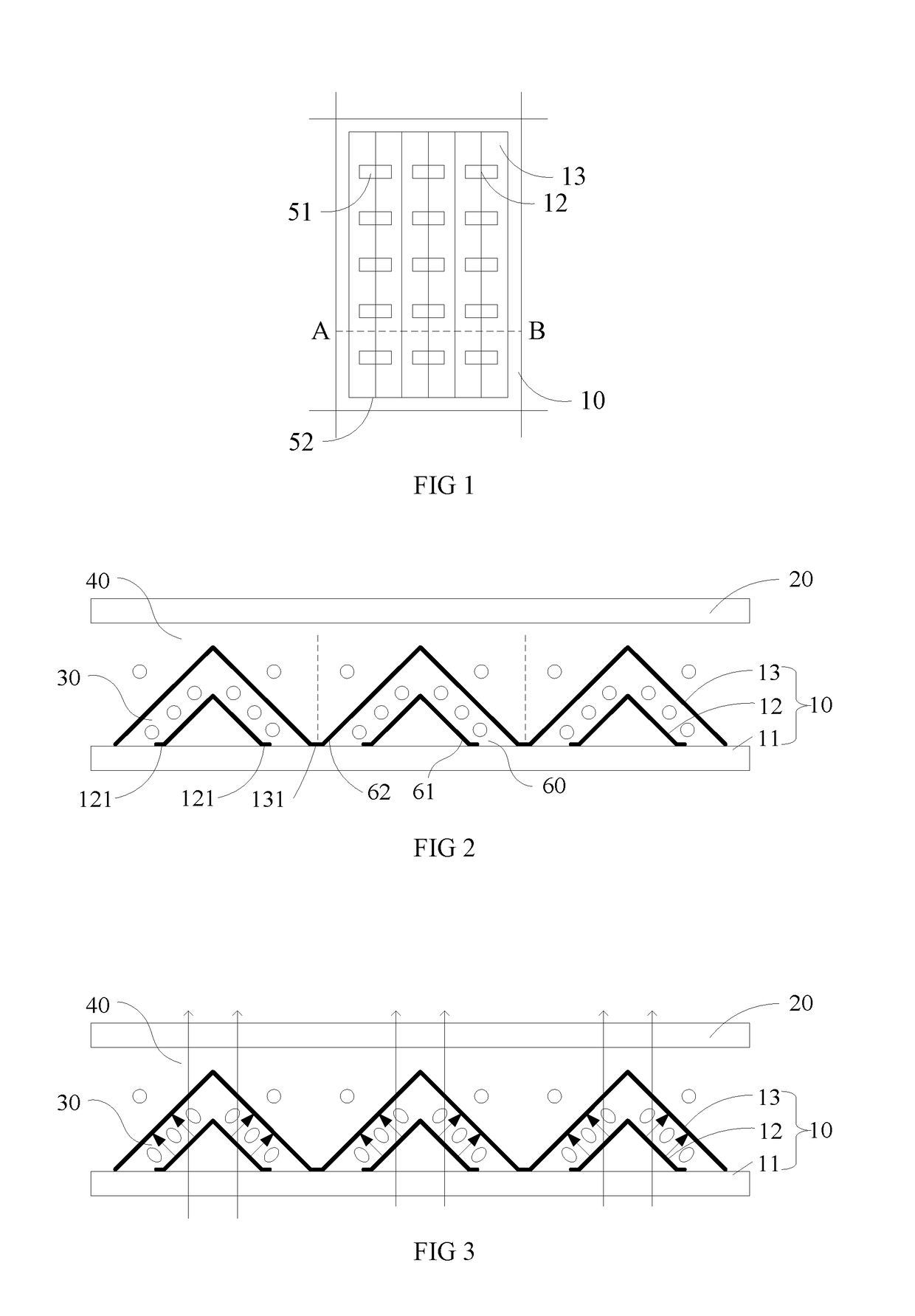
[0070]FIG. 8 is a cross-sectional view of the liquid crystal panel in accordance with a fifth embodiment. The fifth embodiment bases on the first embodiment. A portion of the ripple units 501, 502, and 503 is within the transmission display area, and the other portion of the ripple units 501, 502, and 503 is within the reflective display area. A reflective layer 515 is configured within the first substrate 511, which is below the refle...
third embodiment
[0072]The relationship between ρ and σ may be adjusted such that the phase delay of the light beams passing through the ripple units respectively within the transmission and reflective display area may be the same. The calculations and testing of the relationship between ρ and σ may be understood by referring to the third embodiment, and thus are omitted hereinafter.
[0073]Compared to the third embodiment, the transmission display area and the reflective display area are combined within one ripple unit so as to realize transflective display panel.
[0074]FIG. 9 is a flowchart illustrating the manufacturing method of the blue-phase liquid crystal panel in accordance with the first embodiment.
[0075]In block S110, a first electrode layer, and a second electrode layer are arranged on a first base in sequence to form the first substrate;
[0076]A non-seal first space is arranged between the first electrode layer and the second electrode layer for receiving the blue-phase liquid crystals. The ...
PUM
 Abstract
Description
Claims
Application Information