
Electronic device

a technology of electronic devices and solder points, applied in the direction of printed circuit parts, printed circuit non-printed electric components association, printed circuit final product manufacturing, etc., can solve the problems of large solder points whereby electronic elements are connected to the circuit board, so-called tombstone problems, and reduce the amount of solder materials, so as to prevent the effect of preventing the occurrence of tombstone problems

Active Publication Date: 2018-02-08
SILICONWARE PRECISION IND CO LTD
View PDF2 Cites 0 Cited by
  • Summary
  • Abstract
  • Description
  • Claims
  • Application Information

AI Technical Summary

Benefits of technology

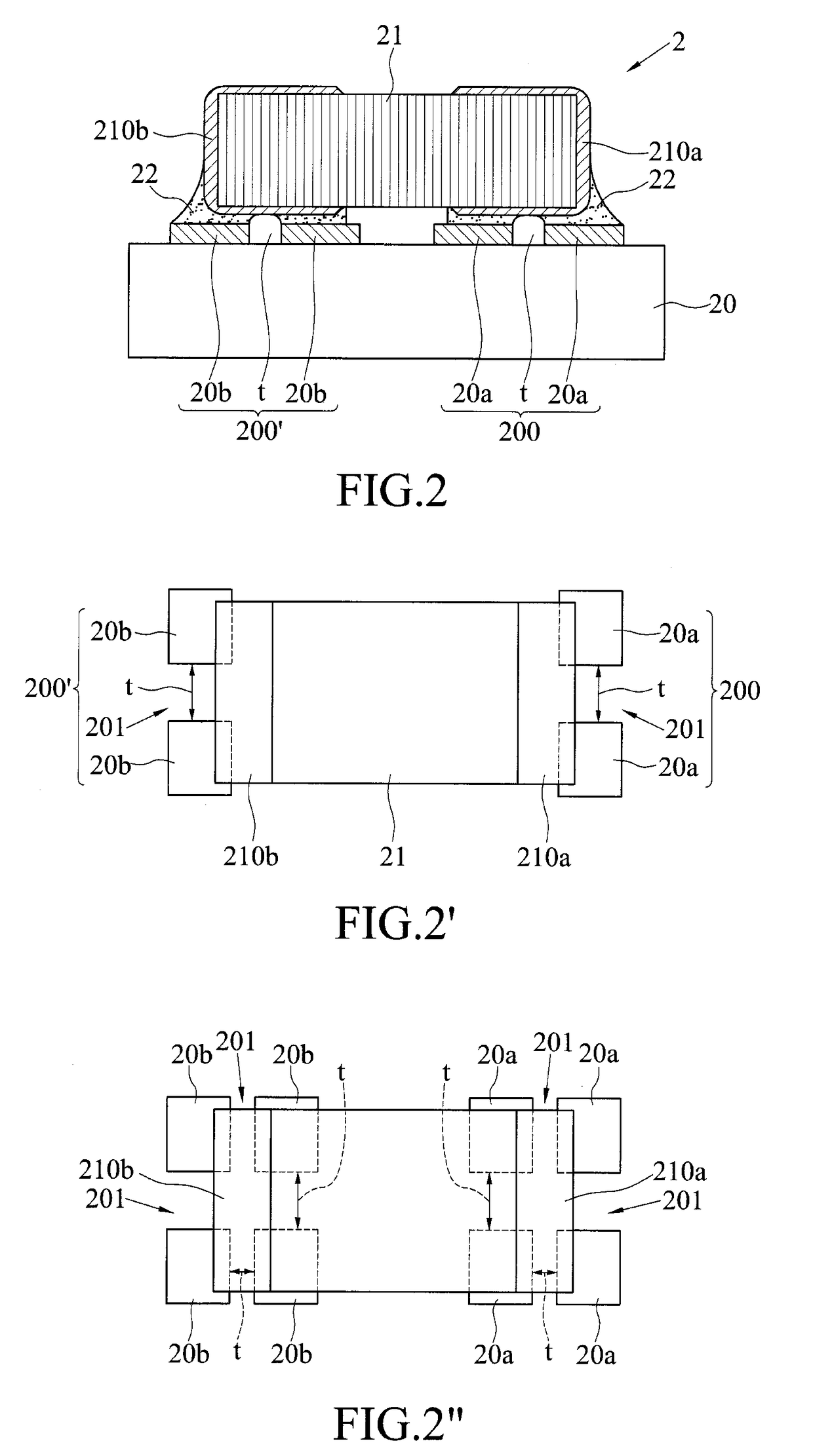
The present invention relates to an electronic device with conductive contacts comprising solder pads and gaps between them, which reduces the bonding area and the amount of solder material used. This control over the solder amount prevents tombstoning and delamination during assembly. Additionally, the reduced amount of solder material transfers less heat to the electronic element, reducing the risk of deformation of the circuit layer. The electronic device is less likely to experience deformation during high temperature reflow process.

Problems solved by technology

In such a scenario, the electronic element disposed on the circuit board using the traditional through hole technology (THT) still has the drawbacks that the electronic element has a size that cannot be further reduced and thereby occupies a large area of the circuit board, and the assembly requires drilling holes on the circuit board based on each of leads.
Further, the solder points whereby the electronic element is connected to the circuit board are also relatively large.
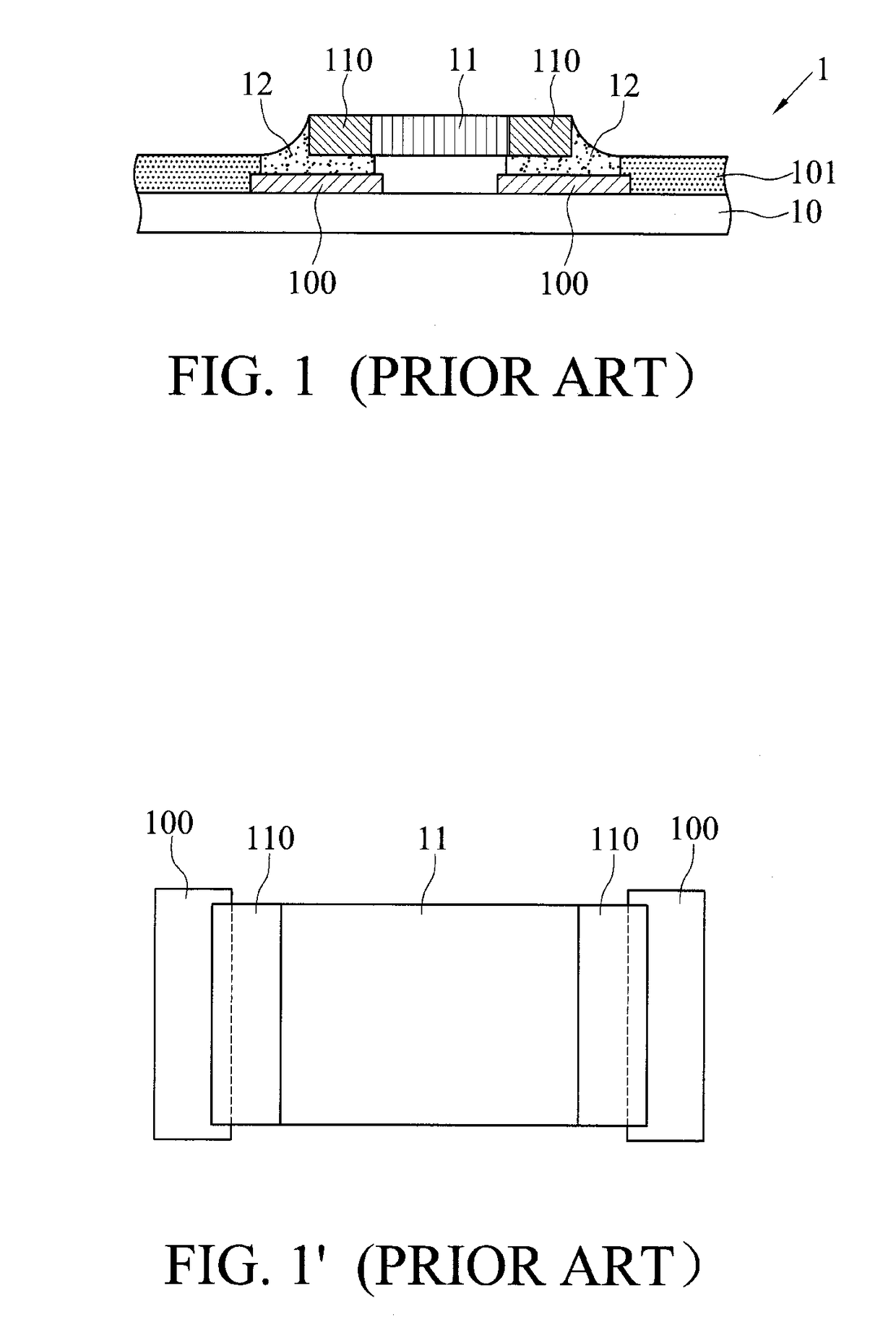
However, during the reflow process, the electronic element 11 may suffer from a shift problem, or have one side tilted, causing a so-called Tombstoning problem, due to the unevenness of the solder paste 12 being applied on the left and right sides.
As a result, the problem of the electronic element 11 that is offset is getting worse.
Furthermore, if the electronic element 11 is packaged using Fan-Out Wafer Level Package (FOWLP), the overall thickness of the circuit structure is generally below 50 um, and there is no rigid circuit board provided as a supporting structure, such that the electrode terminal 110 may likely generate a stress due to its large area, causing delamination of the electronic element 11 during assembly.
The solder paste 12 which has a large size will melt again during the subsequent high temperature process, and a great amount of heat would be transferred to the electronic element 11 from the solder paste 12, thereby increasing the risk of deformation of the circuit layer of the electronic element 11.

Method used


Image

  • Electronic device
  • Electronic device
  • Electronic device

Examples


Embodiment Construction

[0024]The present disclosure is described in the following with specific embodiments, so that one skilled in the pertinent art can easily understand other advantages and effects of the present disclosure from the disclosure of the present disclosure.

[0025]It should be noted that all the drawings are not intended to limit the present disclosure. Various modification and variations can be made without departing from the spirit of the present disclosure. Further, terms, such as “on”, “first”, “second” and “a”, “an” and etc., are merely for illustrative purpose and should not be construed to limit the scope of the present disclosure.

[0026]FIG. 2 is a cross-sectional schematic view of an electronic device 2 according to the present disclosure. As shown in FIG. 2, the electronic device 2 comprises: a circuit board 20 having a plurality of solder pads (which are divided into a plurality of first solder pads 20a and a plurality of second solder pads 20b), and an electronic element 21 dispos...


PUM


Abstract

An electronic device includes a circuit board having a plurality of conductive contacts, and an electronic component disposed on the circuit board and having a plurality of electrode terminals. The conductive contacts include a plurality of solder pads spaced apart from each other, and are coupled to the electrode terminals, respectively. The stress generated by any one of the electrode terminals is distributed to all of the solder pads so as to prevent the electronic component from being offset during an assembly process.

Description

BACKGROUND1. Technical Field[0001]The present disclosure relates to electronic devices, and, more particularly, to an electronic device using surface mounted technology (SMT).2. Description of Related Art[0002]As the technology of fabricating integrated circuit advances, both the design and fabrication of electronic elements favors miniaturization with highly integrated and large scaled circuit, and, as such, a more complete functionality for its product is provided.[0003]In such a scenario, the electronic element disposed on the circuit board using the traditional through hole technology (THT) still has the drawbacks that the electronic element has a size that cannot be further reduced and thereby occupies a large area of the circuit board, and the assembly requires drilling holes on the circuit board based on each of leads. These lead also occupy the area of the opposing sides of the circuit board. Further, the solder points whereby the electronic element is connected to the circu...

Claims


Application Information

Patent Timeline
IPC IPC(8): H05K1/18H05K3/34H05K1/11
CPCH05K1/181H05K3/341H05K1/111H05K2201/09427H05K3/3442H05K2201/09663H05K2201/10636Y02P70/50
Inventor CHEN, LU-YILIU, CHENG-HSIANGLU, CHANG-LUNLIAO, JUN-CHENGCHEN, CHENG-YI
Owner SILICONWARE PRECISION IND CO LTD
Learn More