

Multilayer ceramic capacitor and manufacturing method of multilayer ceramic capacitor
a multi-layer ceramic and manufacturing method technology, applied in the direction of fixed capacitors, stacked capacitors, fixed capacitor details, etc., can solve the problems of insufficient suppression of cracks and insufficient amount of glass components, and achieve the effect of suppressing cracks
- Summary
- Abstract
- Description
- Claims
- Application Information
AI Technical Summary
Benefits of technology
Problems solved by technology
Method used
Image

Examples
embodiment
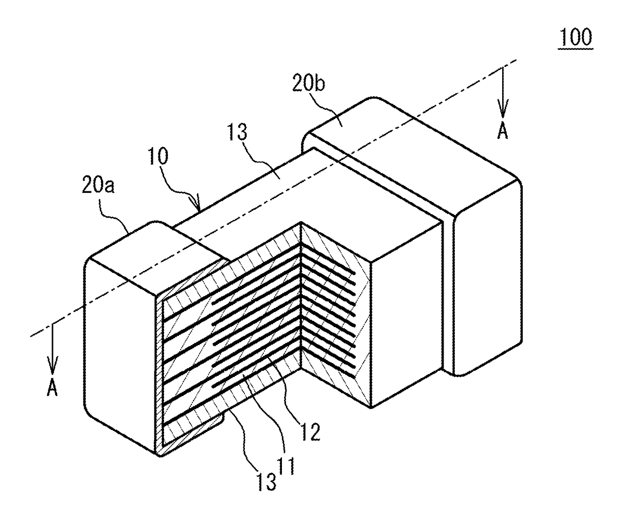
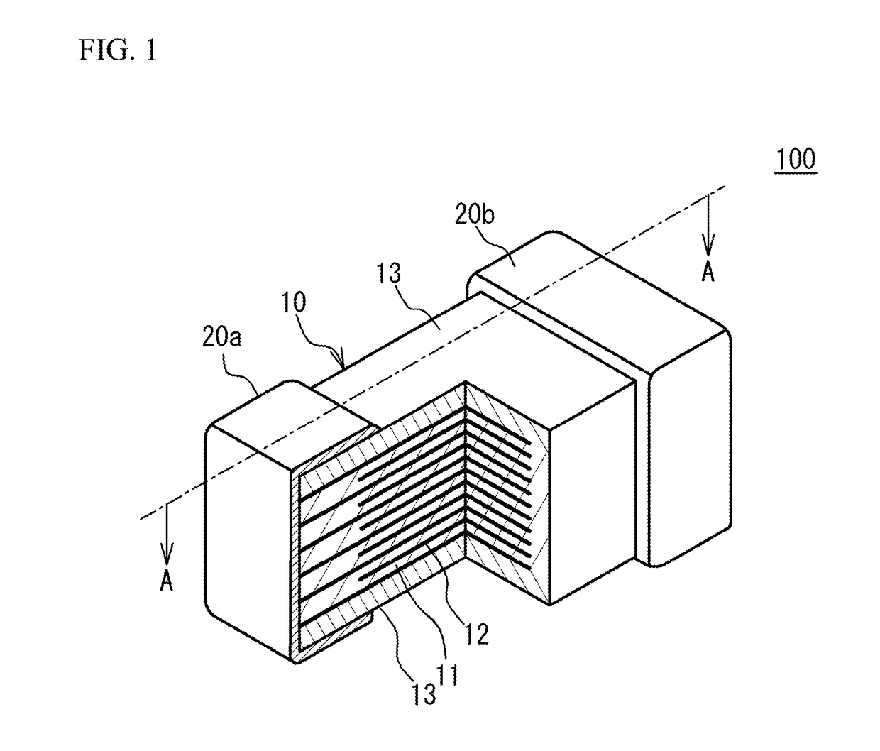
[0016]A description will be given of a multilayer ceramic capacitor. FIG. 1 illustrates a partial perspective view of a multilayer ceramic capacitor 100. As illustrated in FIG. 1, the multilayer ceramic capacitor 100 includes a multilayer chip 10 having a rectangular parallelepiped shape, and a pair of external electrodes 20a and 20b that are respectively provided at two edge faces of the multilayer chip 10 facing each other. Four faces of the multilayer chip 10 other than the two edge faces are referred to as side faces. The external electrodes 20a and 20b extend to the four side faces. However, the external electrodes 20a and 20b are spaced from each other on the four side faces.
[0017]The multilayer chip 10 has a structure designed to have dielectric layers 11 and internal electrode layers 12 alternately stacked. The dielectric layer 11 includes ceramic material acting as a dielectric material. End edges of the internal electrode layers 12 are alternately exposed to a first end fa...
example 1
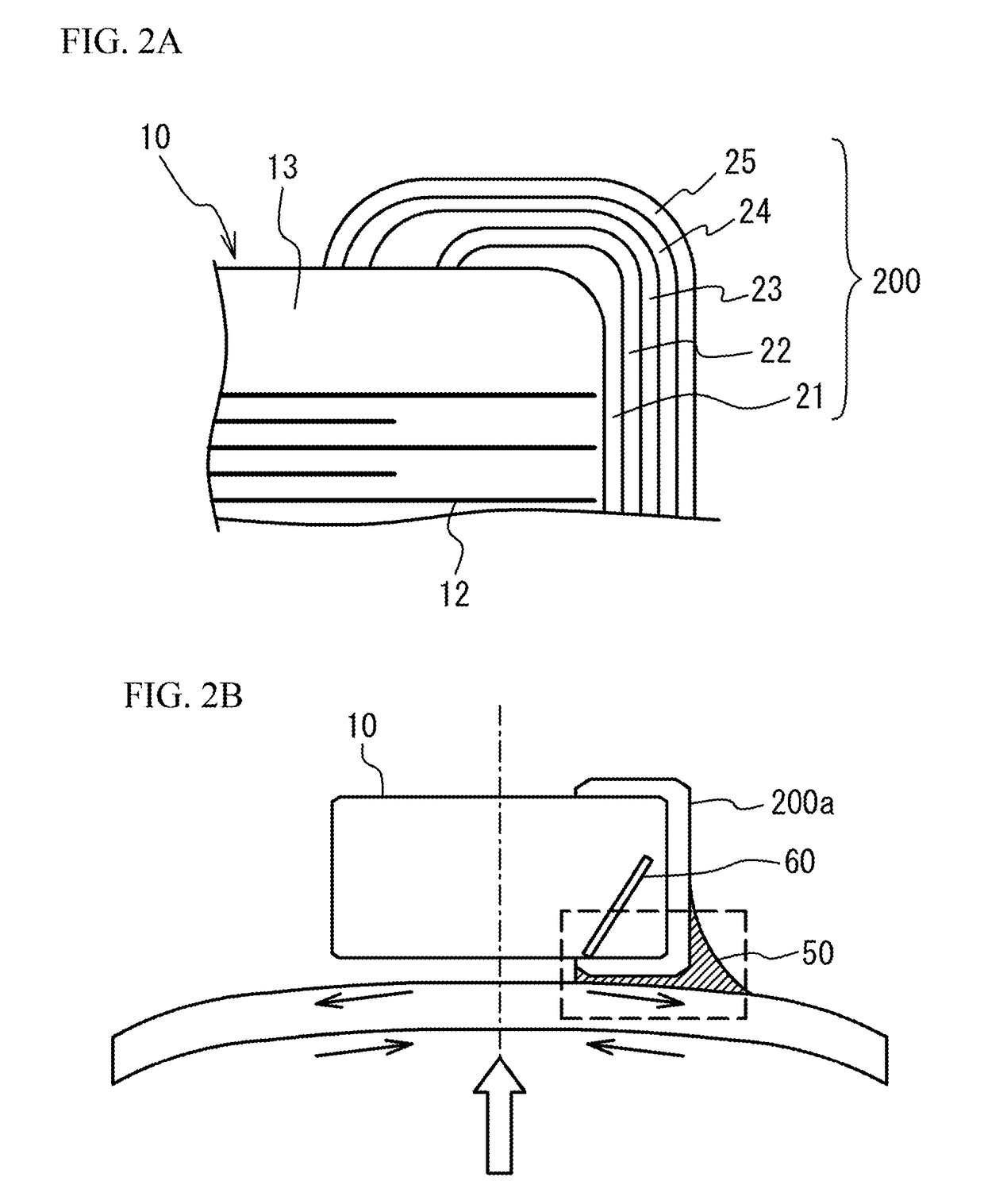
[0044]The multilayer chip 10 baked without forming the external electrodes was prepared. A length, a width and a height of the multilayer chip were 3.2 mm, 1.6 mm and 1.6 mm. The multilayer chip 10 had a capacitance of 10 μF. As illustrated in FIG. 6, the metal paste A including a Cu filler, a glass frit, a binder and a solvent was coated on the both edge faces of the multilayer chip 10 and was dried. Next, the metal paste B including the Cu filler, the glass frit, the binder and the solvent was coated from on the metal paste A to each side face of the multilayer chip 10 and was dried. The metal paste B did not include the glass frit. The sintering of the metal paste B without the glass frit was delayed. Therefore, the diameter of the Cu filler is reduced to approximately 1 / 10 to ½. And, the sintering property was adjusted. Table 1 shows the amount of the glass frit, the material of the binder and the material of the solvent.
TABLE 1PASTE APASTE BCu FILLER3 μm0.5 μmGLASS10 WEIGHT PAR...
example 2
[0049]The multilayer chip 10 (multilayer structure) before the baking was prepared. A length, a width and a height of the multilayer chip 10 were 3.2 mm, 1.6 mm and 1.6 mm when the multilayer chip 10 was obtained from the multilayer structure. A capacitance of the multilayer chip 10 was 10 μF. The metal pastes C including a Ni filler, a co-material, a binder and a solvent was coated on the both edge faces of the multilayer structure, and was dried. Next, the metal paste D including a Ni filler, a binder and a solvent was coated from on the metal paste C to each side face of the multilayer structure and was dried. The metal paste D did not include the co-material. The sintering of the metal paste D was promoted. The sintering property was adjusted by increasing the diameter of the Ni filler to twice to five times. Table 5 shows amount of the mixed co-material, the material of the binder and the material of the solvent.
TABLE 5PASTE CPASTE DNi FILLER0.5 μm1 μmGLASS25 WEIGHT PART0 WEIGH...
PUM
| Property | Measurement | Unit |
|---|---|---|
| Dielectric polarization enthalpy | aaaaa | aaaaa |
Abstract
Description
Claims
Application Information