

Reduction of solder interconnect stress
a solder interconnect and stress technology, applied in the field of electronic devices or electronic packages, can solve the problems of physical or dimensional expansion of the heat of the processing device, and the inability to expand the processing device and the interposer uniformly
- Summary
- Abstract
- Description
- Claims
- Application Information
AI Technical Summary
Benefits of technology
Problems solved by technology
Method used
Image

Examples
Embodiment Construction
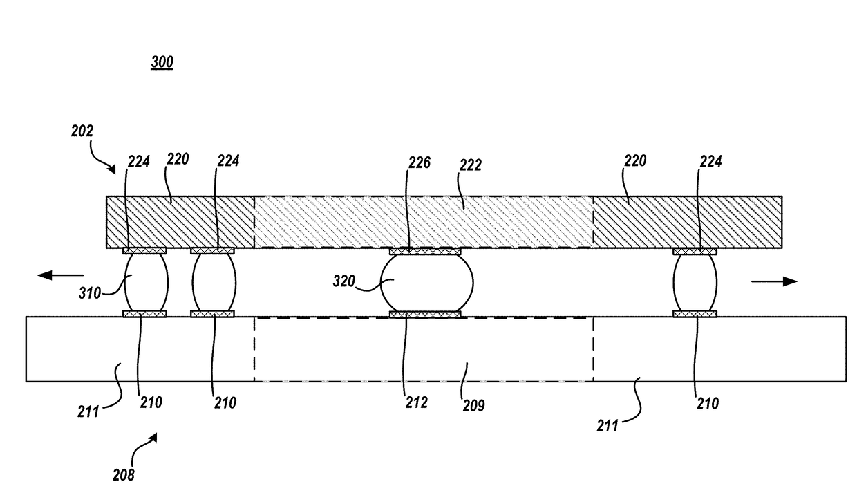
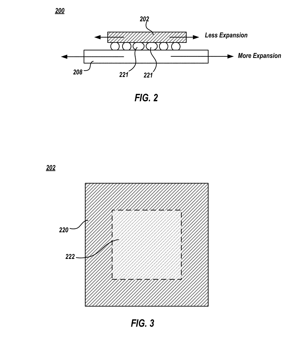
[0001]Embodiments of the present invention generally relate to electronic devices or electronic packages and more specifically to the reduction of solder interconnect stress.
DESCRIPTION OF THE RELATED ART
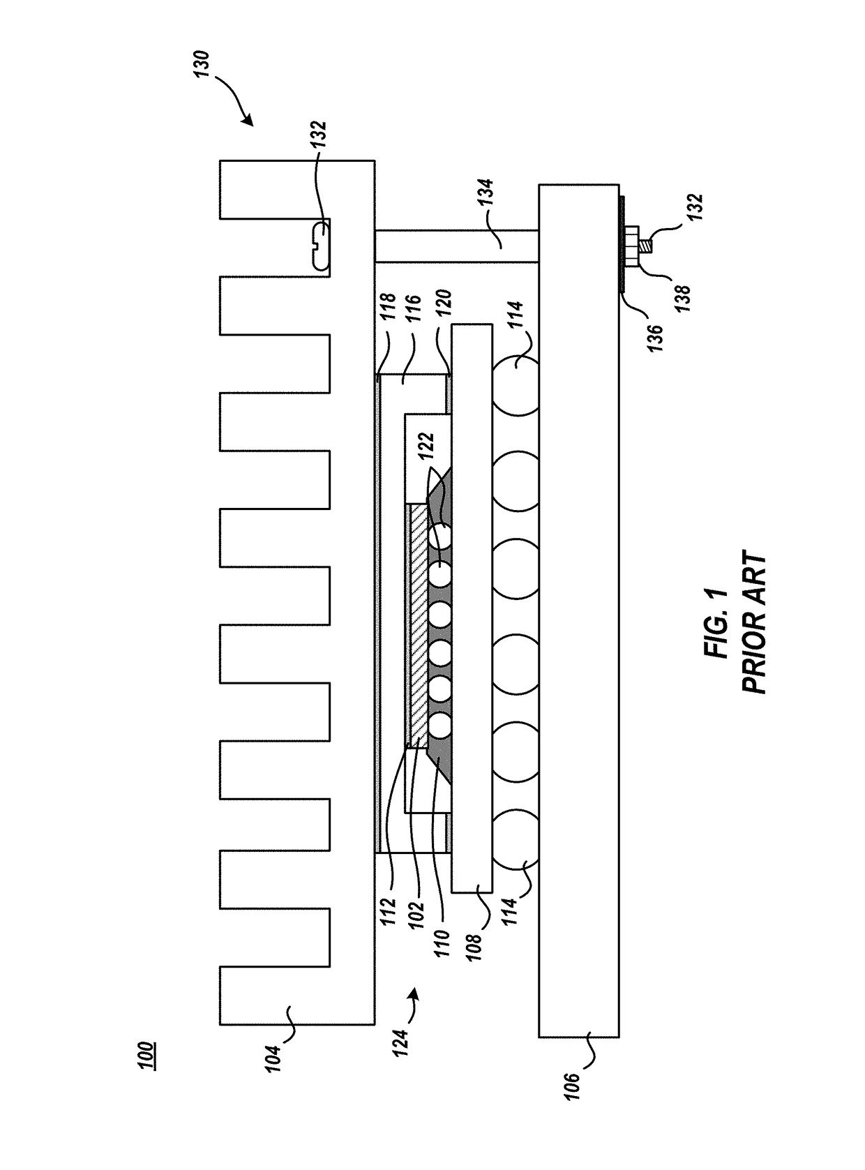
[0002]An electronic package may include an integrated circuit (IC) chip, semiconductor die, processor, and the like, herein referred to as a processing device, packaged onto a carrier or substrate, herein referred to an interposer. The processing device may be encapsulated by a cover having high thermal conductivity. A heat sink may be thermally connected to the cover to cool the processing device during operation of the electronic device where electrical energy is used by the processing device which results in the heating of the processing device. In some instances, there is no cover and the heat sink is attached directly to the processing device. The heat sink generally removes heat from the processing device causing the processing device to operate at a lower temperature. The ele...
PUM
 Abstract
Description
Claims
Application Information