

Polishing composition for silicon wafer and polishing method
a technology of silicon wafer and composition, applied in the direction of lapping machines, manufacturing tools, other chemical processes, etc., can solve the problems of increasing the adverse effect of the performance of the semiconductor device, and achieve the effect of preventing metal contamination and reducing the lpd
Active Publication Date: 2018-03-08
FUJIMI INCORPORATED
View PDF1 Cites 5 Cited by
- Summary
- Abstract
- Description
- Claims
- Application Information
AI Technical Summary
Benefits of technology
Technical effects: This patent describes a new technology that allows for better control and management of electronic devices. This technology involves the use of special chips that can communicate with each other and help to synchronize the movement and behavior of the devices. Overall, this invention improves the efficiency and reliability of electronic devices.
Problems solved by technology
Therefore, a case where substrate surface defects of nanometer scale, which have not been treated as problems heretofore, adversely affect on the performance of the semiconductor device has increased.
Method used
View moreImage
Smart ImageViewing Examples

Examples
examples
[0072]Next, the present invention is more specifically described with reference to Examples and Comparative Examples.
Login to View More PUM
 Abstract
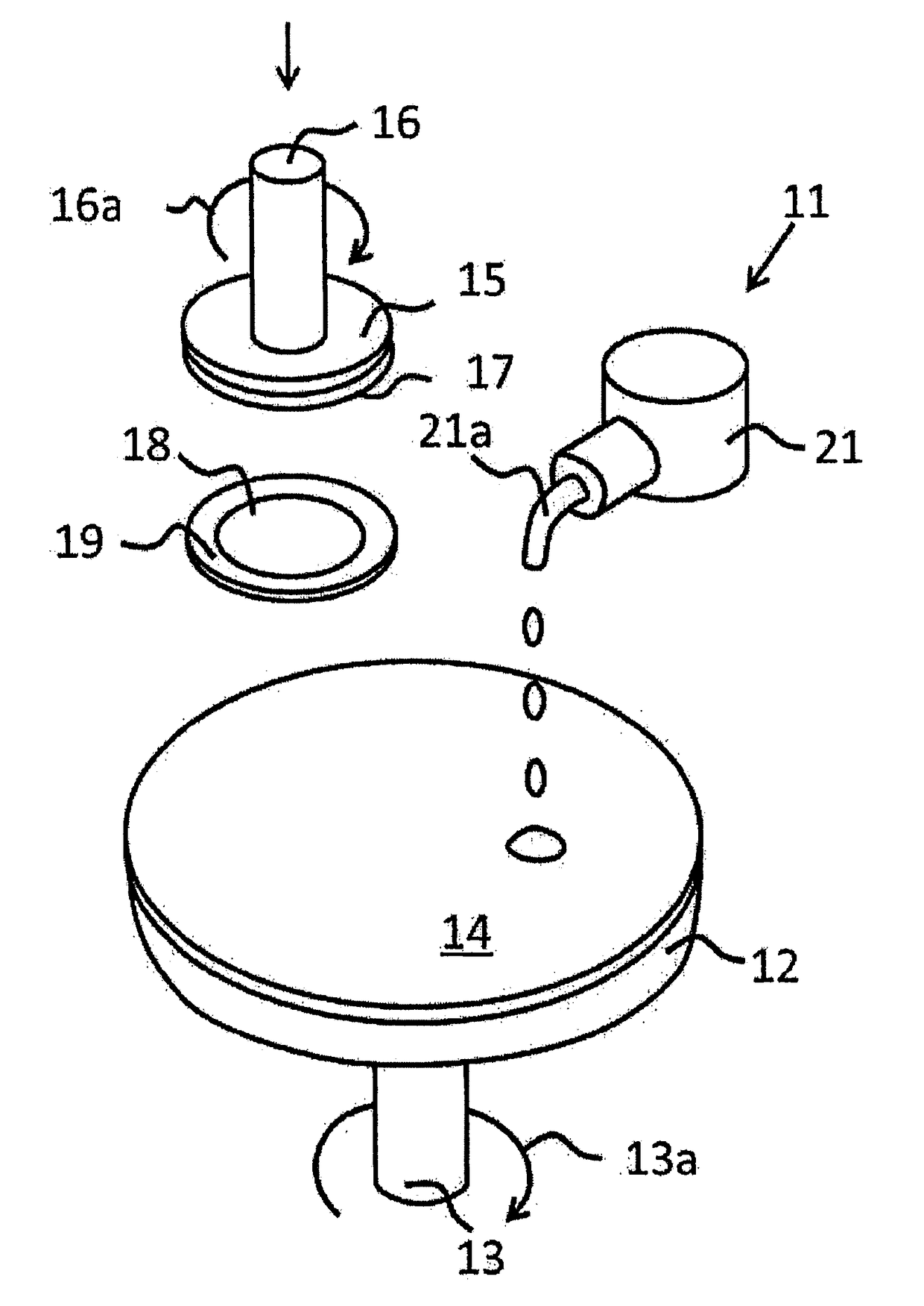
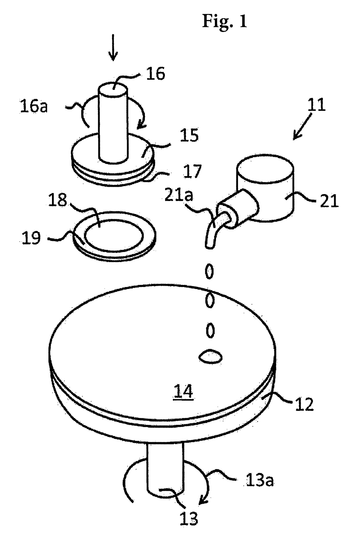
To perform polishing while reducing an LPD and preventing contamination with metals, particularly nickel and copper, in final polishing of a silicon wafer. A polishing composition contains abrasives, a water-soluble polymer, a basic compound, a chelating agent, and water, in which, when the particle diameter equivalent to a particle diameter at a cumulative volume of 10% from a smaller particle diameter side is defined as D10, the particle diameter equivalent to a particle diameter at a cumulative volume of 50% from the smaller particle diameter side is defined as D50, and the particle diameter equivalent to a particle diameter at a cumulative volume of 90% from the smaller particle diameter side is defined as D90 in a particle size distribution of particles present in the polishing composition, a value of a coarse particle frequency parameter A defined by (Expression 1) illustrated below is less than 1.7, A=(D90−D50) / (D50−D10) and the polishing composition is used for final polishing in silicon wafer polishing.
Description
TECHNICAL FIELD[0001]The present invention relates to a polishing composition for silicon wafer and particularly relates to a polishing composition and a polishing method for use in final polishing of a silicon wafer.BACKGROUND ART[0002]In a semiconductor device for use in a computer, miniaturization of the wiring width referred to as a design rule has advanced year after year in order to realize a higher integration and an increase in speed. Therefore, a case where substrate surface defects of nanometer scale, which have not been treated as problems heretofore, adversely affect on the performance of the semiconductor device has increased. Therefore, the importance of overcoming the substrate surface defects with nanometer scale has increased.[0003]Among semiconductor substrates, a polishing composition containing silica particles and a water-soluble polymer is preferably used for silicon wafer polishing. When a silicon wafer is polished with a polishing composition disclosed in Pat...
Claims
Login to View More Application Information
Patent Timeline
 IPC IPC(8): C09G1/02C09K3/14H01L21/304
CPCC09G1/02C09K3/1463H01L21/304H01L21/02024B24B37/044C09K3/1409B24B37/00
InventorTSUCHIYA, KOHSUKEMOMOTA, SATOSHI
OwnerFUJIMI INCORPORATED