Six-degree-of-freedom displacement measurement method for exposure region on silicon wafer stage

Active Publication Date: 2018-03-22
BEIJING U PRECISION TECH +1
View PDF0 Cites 0 Cited by
  • Summary
  • Abstract
  • Description
  • Claims
  • Application Information

AI Technical Summary

Benefits of technology

[0012]Compared with the technical solution in the prior art, the present invention has the following advantages and outstanding technical effects: in the technical solution provided by the present invention, the six-degree-of-freedom displacement of the exposure region at any time during the movement of the wafer s

Problems solved by technology

However, the reading head of the existing planar grating measurement system is mostly placed on the movable platform, such that a displacement of a fixed point on the movable platform is measured, but th

Method used


Image

  • Six-degree-of-freedom displacement measurement method for exposure region on silicon wafer stage
  • Six-degree-of-freedom displacement measurement method for exposure region on silicon wafer stage

Examples


Embodiment Construction

[0017]Hereinafter, the implementations of the present invention are further explained in detail in connection with the accompanying drawings.

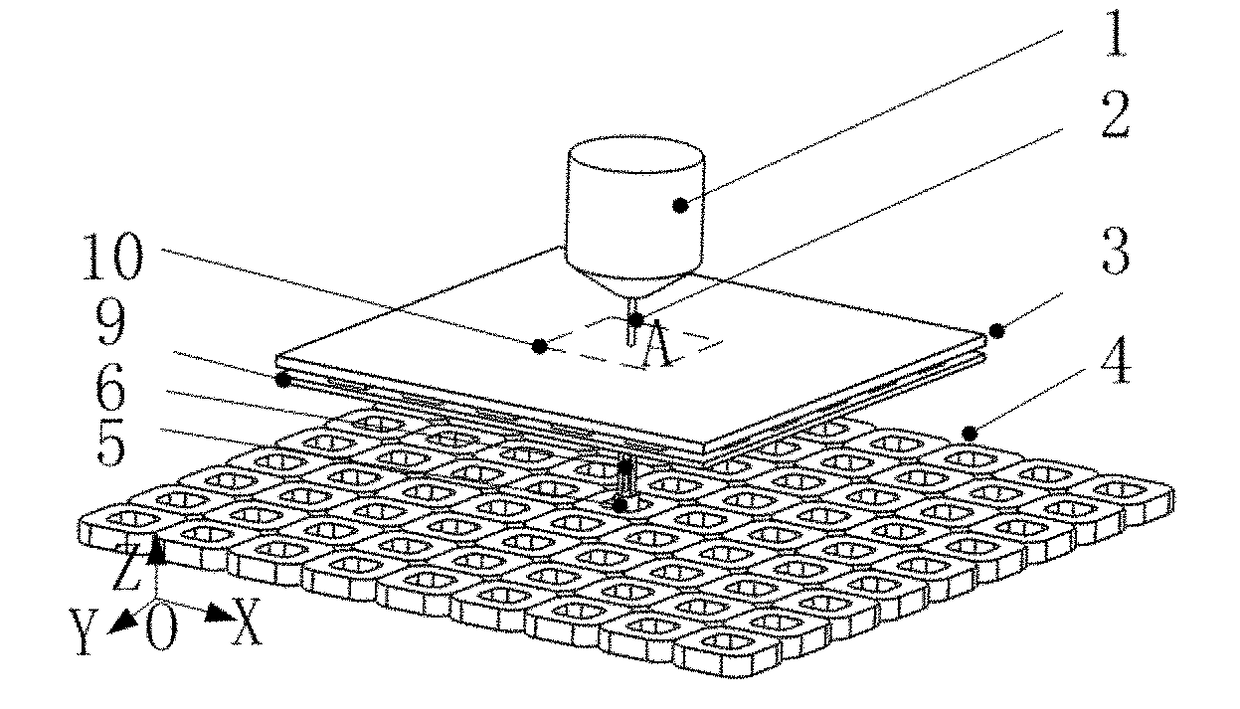
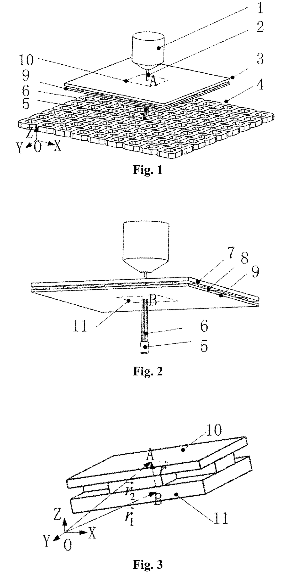
[0018]FIG. 1 is a schematic view showing an embodiment of the six-degree-of-freedom displacement measurement method for the exposure region on the wafer stage provided by the present invention. The wafer stage comprises a coil array 4 and a movable platform 3, and the coil array 4 consists of coils arranged in a plane. In the present embodiment, square coils are used. FIG. 2 is a schematic view showing the measurement device in the embodiment. The movable platform 3 comprises a permanent magnet array 8 and a back plate 7, and the permanent magnet array 8 is bonded to the bottom of the back plate 7. The permanent magnet array 8 employs a two-dimensional permanent magnet array, and in this embodiment, a two-dimensional halbach-type permanent magnet array is used. A planar grating 9 is fixed below the permanent magnet array 8 such that the measure...


PUM


Abstract

A six-degree-of-freedom displacement measurement method for an exposure region on a wafer stage, the wafer stage comprises a coil array and a movable platform. A planar grating is fixed below a permanent magnet array of the movable platform. A reading head is fixed in a gap of the coil array. A measurement region is formed on the planar grating by an incident measurement light beam of the reading head. The reading head measures the six-degree-of-freedom displacement of the measurement region, so that the six-degree-of-freedom displacement of the exposure region is obtained through calculation. In the method, the six-degree-of-freedom displacement of the exposure region at any time is measured; the measurement complexity is reduced and the measurement precision is improved, and especially, the six-degree-of-freedom displacement of the exposure region can be precisely measured at any time even if the movable platform has high flexibility.

Description

TECHNICAL FIELD[0001]The present invention relates to a six-degree-of-freedom displacement measurement method for an exposure region on a wafer stage, which may be applied to a semiconductor lithography machine and belongs to the technical field of semiconductor manufacturing equipment.BACKGROUND ART[0002]During an exposure process of a lithography machine, a wafer is divided into multiple fields of view to be exposed respectively. During an exposure process of a field of view on the wafer, an exposure image is projected onto the wafer by the lens to form an exposure region. In order to ensure the exposure accuracy, the wafer stage is required to be leveled and focused, and to adjust the horizontal position, so as to ensure the relative position and angle between the exposure region and the lens. Thus, six-degree-of-freedom displacement measurement of the exposure region is particularly important. When this field of view is exposed, the wafer stage moves, so that the next field of v...

Claims


Application Information

Patent Timeline
IPC IPC(8): G01B11/14G03F9/00
CPCG01B11/14G03F9/7046G01B11/272G01B11/002G03F7/70775G01D5/38G03F7/70758
Inventor ZHU, YUZHANG, MINGCHEN, ANLINCHENG, RONGYANG, KAIMINGLIU, FENGSONG, YUJINGZHI, FANHU, JINCHUNXU, DENGFENGMU, HAIHUAHU, CHUXIONG
Owner BEIJING U PRECISION TECH
Why Eureka
Try Eureka