Processing method for wafer

Active Publication Date: 2018-03-22
DISCO CORP
View PDF2 Cites 4 Cited by
  • Summary
  • Abstract
  • Description
  • Claims
  • Application Information

AI Technical Summary

Benefits of technology

[0009]In the processing method for a wafer according to the one aspect of the present invention, the surface protective tape is stuck in a heated state to the front face of the wafer. The surface protective tape is configured from a base material and a glue layer, and if the glue layer is heated, then it is softened and the close contactness thereof with the front face of the wafer enhances. Consequently, when the wafer is divided into individual

Problems solved by technology

Although, at such a step as described above, when grinding is being performed, cracks extend from the modified layer and gaps along which the wafer is to be divided are formed, the gaps are very narrow.
Since a corner portion of a chip is vulnerable to impact, if corner portions are contacted with each other and acted upon by impact, then the chips are likely to suffer from damage such as chipping or cracking.
Since any damaged chip is unacceptable, contact between corner

Method used


Image

  • Processing method for wafer
  • Processing method for wafer
  • Processing method for wafer

Examples


Example

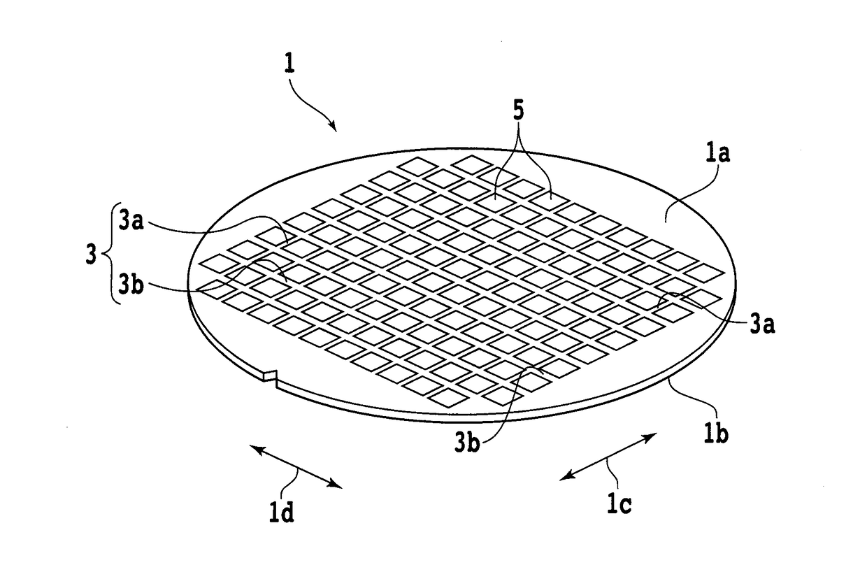
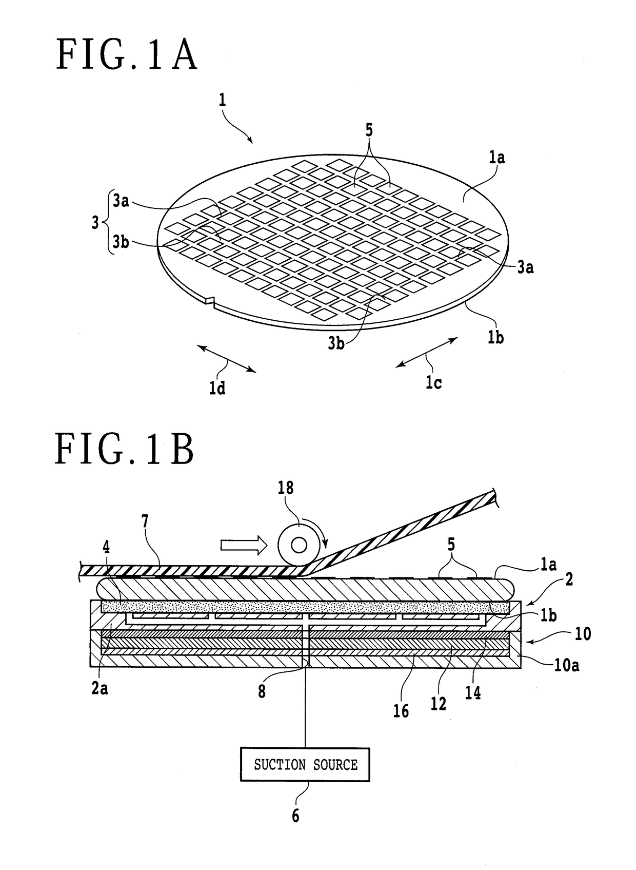
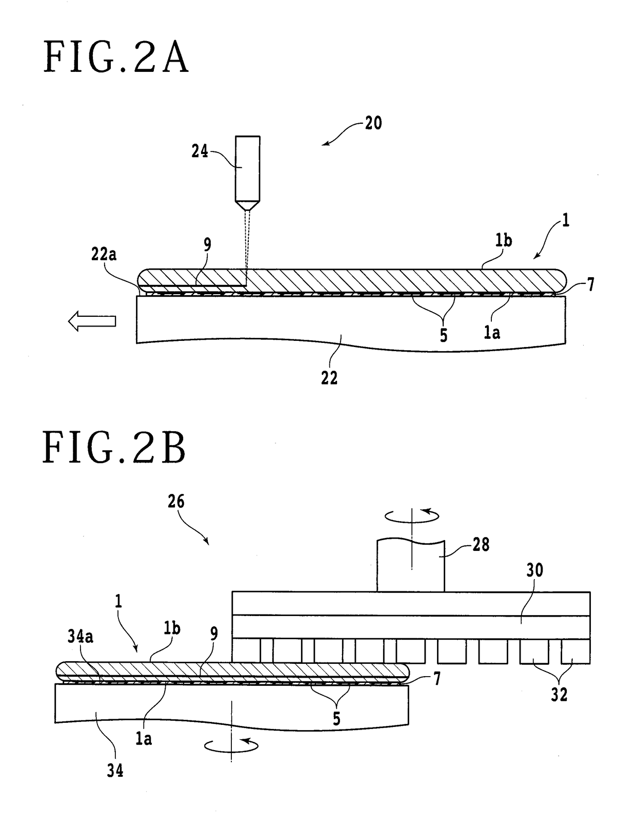
[0017]An embodiment of the present invention is described. A wafer that is a workpiece of a processing method according to the present embodiment is described. FIG. 1A is a perspective view depicting an example of the wafer. The wafer 1 that is a workpiece in the processing method according to the present embodiment is a substrate made of such a material as, for example, silicon, silicon carbide (SiC) or some other semiconductor or of a material such as sapphire, glass or quartz. A front face 1a of the wafer 1 is partitioned into a plurality of regions by streets 3 arrayed in a grid pattern. The streets 3 include first streets 3a extending in a first direction 1c and second streets 3b extending in a second direction 1d crossing with the first direction 1c. In each of the regions partitioned by the streets 3, a device 5 such as an IC is formed. The wafer 1 is finally divided along the streets 3 to form individual chips.

[0018]Now, a processing method for the wafer 1 according to the p...


PUM

PropertyMeasurementUnit
Transparencyaaaaaaaaaa

Abstract

A wafer has a front face that is partitioned by a plurality of streets crossing with each other into a plurality of regions in each of which a device is formed. A surface protective tape is adhered to the front face of the wafer. Then a laser beam having a wavelength transparent to the wafer is irradiated along the streets from a rear face side of the wafer to form a modified layer inside the wafer. Then the wafer is ground from the rear face side to thin the wafer. When the surface protective tape is applied, the surface protective tape is heated. When the modified layer is formed, cracks extend from the modified layer to the front face of the wafer. When ground, the wafer is divided into individual chips with the cracks serving as boundaries.

Description

BACKGROUND OF THE INVENTIONField of the Invention[0001]The present invention relates to a processing method for a wafer.Description of the Related Art[0002]In a step of processing a wafer to fabricate a chip or the like, in order to thin a wafer having devices formed on the front face thereof, for example, the rear face side of the wafer is ground. Thereafter, the wafer is divided to form individual chips. When the wafer is divided, a modified layer that serves as a start point of division is formed in the wafer along latticed streets by a laser processing apparatus, and then external force is applied to the wafer such that a crack extends in the thicknesswise direction of the wafer from the modified layer.[0003]For such a fabrication step of chips as described above, for example, as indicated in PCT Patent Publication No. WO03 / 077295, a step of carrying out grinding of the rear face side and division of a wafer into chips at the same time is investigated. At this step, a modified l...

Claims


Application Information

Patent Timeline
IPC IPC(8): H01L21/78H01L21/683
CPCH01L21/78H01L21/6836H01L21/304H01L21/67132H01L2221/68327H01L2221/6834H01L21/786H01L21/76B23K26/0093B23K26/53
Inventor AGARI, MASAMITSUTEWOO, BAE
Owner DISCO CORP
Why Eureka
Try Eureka