Check patentability & draft patents in minutes with Patsnap Eureka AI!

Resistive Memory Apparatus

Active Publication Date: 2018-03-29
IBM CORP
View PDF2 Cites 1 Cited by
  • Summary
  • Abstract
  • Description
  • Claims
  • Application Information

AI Technical Summary

Benefits of technology

The invention provides an apparatus with a memory cell unit comprising a variable-resistance channel component and a plurality of resistive memory elements. The apparatus includes control circuitry that can apply control signals to the gate and supply terminals in a read mode to select one or more memory elements. The control circuitry can also apply a control signal to deselect any remaining memory elements in the read mode. The technical effects of the invention are improved performance and reliability of the memory cell unit, as well as increased efficiency in the read mode with advanced selection capabilities.

Problems solved by technology

It is widely believed that such BEOL-compatible 3D efforts cannot lead to a significant number of memory layers (e.g. >5 layers) due to challenges associated with microfabrication as well as difficulties associated with addressing individual devices.
Moreover, for reliable operation, prior devices are restricted to storing 1-bit per cell because resistive memory cells are subject to resistance variations such as resistance drift over time drift, substantial flicker noise, and resistance that varies with ambient temperature.
Such effects inhibit reliable readback for multilevel operation where the resistance levels of different cell-states are more closely packed, and therefore harder to distinguish in the presence of stochastic resistance variations.
These problems present a significant challenge in the drive to increase storage densities and areal efficiency of resistive memory devices.

Method used


Image

  • Resistive Memory Apparatus
  • Resistive Memory Apparatus
  • Resistive Memory Apparatus

Examples


first embodiment

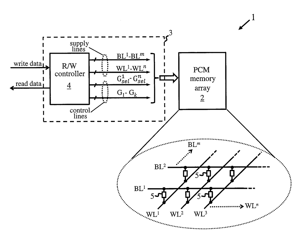
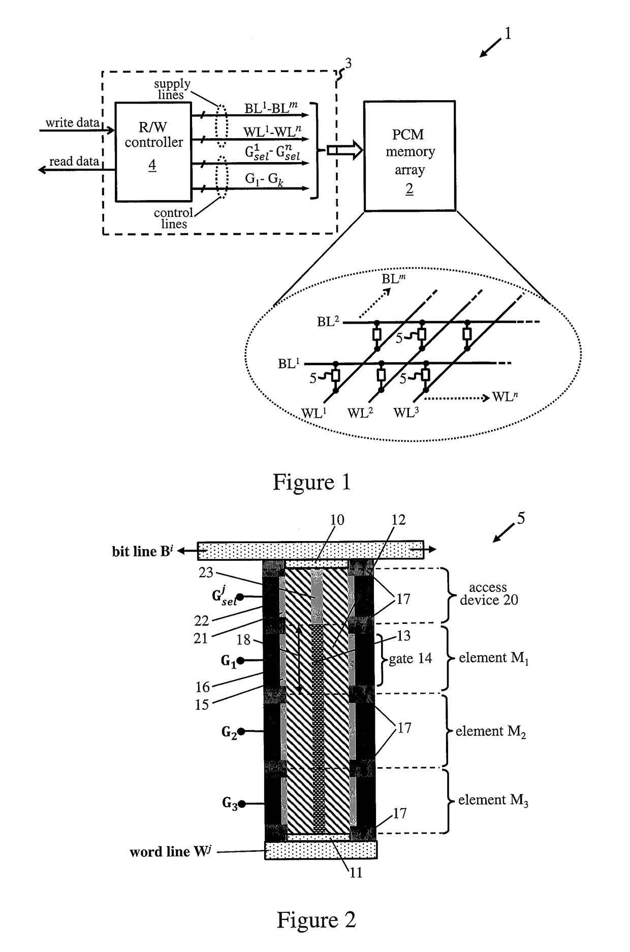
[0028]FIG. 2 is a schematic cross-sectional view of a PCM cell unit 5 in a The cell unit 5 is arranged between first and second supply terminals formed here by ohmic contacts 10 and 11 and the adjoining regions of the bit line Bi and word line Wj connected to the cell unit. A variable-resistance channel component 12 extends between the two supply terminals. In this embodiment, channel component 12 contacts both supply terminals and is formed as an elongate annulus of semiconductor material. A plurality k of PCM memory elements Mk are arranged along the channel component 12. In the simple example shown, k=3. Each memory element M1 to M3 comprises a PCM material 13 which extends along a respective segment of the channel component in contact therewith. Successive channel segments are demarcated by the dashed lines in the figure. In this embodiment, the PCM material of elements M1 to M3 is disposed within the annular channel component 12 and is formed as a continuous core of PCM materi...

second embodiment

[0038]FIG. 7 is a schematic cross-sectional view of a PCM cell unit. The cell unit 30 of this embodiment corresponds generally to that of FIG. 4, and corresponding components are indicated by like reference numerals. Each memory element Mk here includes a fixed-resistance component 31 extending along the respective channel segment in contact with the PCM material 32 on an opposite surface of the PCM material to the channel segment. In this example, the fixed-resistance component 31 is formed as a continuous core component and the PCM material 32 forms an annulus around the core component 31. The core component 31 is a moderate conductor which may be formed, for example, of a metal nitride or a doped semiconductor such as doped polysilicon. The material is selected such that core component 31 has a resistance which is between that of the amorphous and crystalline regions of the PCM material at the read voltage Vread as illustrated schematically in FIG. 8. Core component 31 thus provi...


PUM


Abstract

Apparatus including: memory cell unit(s) having a variable-resistance channel component (CC) extending between first and second supply terminals for supplying read and write (R / W) signals to the unit in respective R / W modes, and resistive memory elements (RMEs) arranged along the CC, RME includes resistive memory material (RMM), extending along a respective channel segment (CHS) of the CC in contact therewith, in which respective lengths along that CHS of high- and low-resistance regions is variable in write mode, and a gate terminal provided on that CHS for controlling resistance of the CHS in response to control signal(s) (CS) applied to the gate terminal; and circuitry configured to apply the CS such that, in read mode, a RME(s) is selected by applying a CS producing CHS with resistance between the resistance regions of the RMM; and remaining RME(s) are deselected by applying CS producing CHS having resistance less than the low-resistance region.

Description

BACKGROUND[0001]The present invention relates generally to resistive memory apparatus, and more particularly to apparatus comprising one or more memory cell units containing a plurality of resistive memory elements in which a resistive memory material is used for information storage.[0002]This section is intended to provide a background or context to the invention disclosed below. The description herein may include concepts that could be pursued, but are not necessarily ones that have been previously conceived, implemented or described. Therefore, unless otherwise explicitly indicated herein, what is described in this section is not prior art to the description in this application and is not admitted to be prior art by inclusion in this section.[0003]Resistive memory cells such as phase-change memory (PCM) cells use a resistive memory material for storage of information. The resistance of such cells can be programmed via a progamming (or “write”) operation that changes the relative ...

Claims


Application Information

Patent Timeline
IPC IPC(8): G11C13/00
CPCG11C13/0004G11C13/0069G11C13/004
Inventor CZORNOMAZ, LUKASDESHPANDE, VEERESH VIDYADHARJONNALAGADDA, VARA SUDANAN PRASADKOELMANS, WABESEBASTIAN, ABU
Owner IBM CORP
Features
  • R&D
  • Intellectual Property
  • Life Sciences
  • Materials
  • Tech Scout
  • Unparalleled Data Quality
  • Higher Quality Content
  • 60% Fewer Hallucinations
Learn More