Method of fabricating x-ray absorbers for lowenergyx-ray spectroscopy

Inactive Publication Date: 2018-03-29
NASA
View PDF1 Cites 5 Cited by
  • Summary
  • Abstract
  • Description
  • Claims
  • Application Information

AI Technical Summary

Benefits of technology

[0006]An aspect of the invention is a large, thin e-beam evaporated absorber with one or more stems electroplated and a relatively shallow angle to the absorber at the stems;
[0007]Another aspect of the invention is one or more electroplated stem(s) connected to, and with a relatively shallow angle to, a thin e-beam evaporated absorber that is large enough to sense low-energy electrons at or below 1 keV.
[0008]The present invention relates to a method of forming low-energy x-ra

Problems solved by technology

While, higher energy absorbers can be fairly thick titanium/gold or titanium/gold/bismuth, these thick absorbers are unusable below 1 keV.
While, higher energy absorbers can be fairly thick metal bilayers or tri-layers, e.g. titanium/gold or titanium/gold/bismuth, these thick absorbers are unusable below 1 keV.
Unfortunately, the microfabrication techniques traditionally used for thick absorbers (>1 μm thick) in state-of-the-art high-energy x-ray microcalorimeters are unusable for manufacturing thinner

Method used


Image

  • Method of fabricating x-ray absorbers for lowenergyx-ray spectroscopy
  • Method of fabricating x-ray absorbers for lowenergyx-ray spectroscopy
  • Method of fabricating x-ray absorbers for lowenergyx-ray spectroscopy

Examples


Embodiment Construction

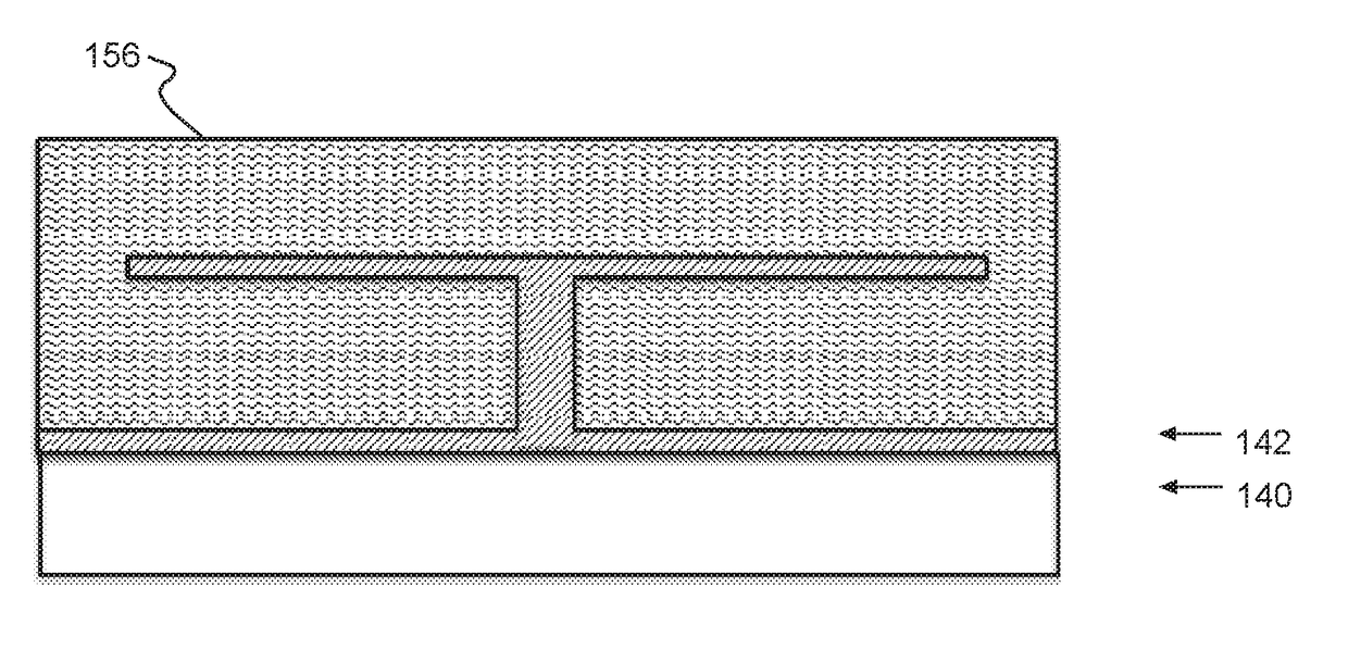
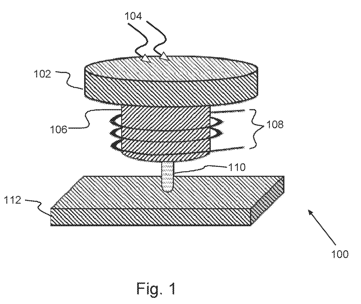
[0013]Turning now to the drawings and more particularly FIG. 1 shows an example of an ideal large, thin low-energy x-ray pixel 100 for use in high-resolution x-ray microcalorimeters with an absorber 102 formed on a wafer, e.g., a semiconductor wafer, according to a preferred embodiment of the present invention. For sensing low-energy x-rays 104 striking the preferred absorber 102, the preferred absorber 102 is much larger and thinner than prior higher energy x-ray absorbers. An underlying sensor 106 is in intimate contact with, and senses heat generated in, the absorber 102. A stem extending through the sensor 106 to the absorber 102 may pass heat from the absorber 102 to the sensor 106, which couples 108 the sensor 106 response to readout electronics (not shown). The stem of this example also acts as thermal link 110 coupling the sensor 106 to a thermal bath 112, e.g., an underlying semiconductor substrate supporting the pixel 100.

[0014]Incoming energy (from low energy x-rays) 104 ...


PUM


Abstract

A method of forming low-energy x-ray absorbers. Sensors may be formed on a semiconductor, e.g., silicon, wafer. A seed metal layer, e.g., gold, is deposited on the wafer and patterned into stem pads for electroplating. Stems, e.g., gold, are electroplated from the stem seed pads through a stem mask. An absorber layer, e.g., gold, is deposited on the wafer, preferably e-beam evaporated. After patterning the absorbers, absorber and stem mask material is removed, e.g., in a solvent bath and critical point drying.

Description

ORIGIN OF THE INVENTION[0001]The invention described herein was made by an employee of the United States Government, and may be manufactured and used by or for the Government for governmental purposes without the payment of any royalties thereon or therefor.BACKGROUND OF THE INVENTIONField of the Invention[0002]The present invention is generally related to x-ray spectroscopy and more particularly to fabricating x-ray absorbers for sensing low energy x-rays, especially in high-resolution x-ray microcalorimeters used in spaceborne x-ray spectroscopy applications.Background Description[0003]For future rocket-based spectroscopy missions National Aeronautics and Space Administration (NASA) requires high-resolution x-ray microcalorimeters with large pixel viewing areas, capable of low-energy measurements below one thousand electron volts (<1 keV). State of the art microfabrication techniques have been used successfully to fabricate higher energy suspended x-ray absorbers, optimized for...

Claims


Application Information

Patent Timeline
IPC IPC(8): H01L39/24H01L21/027G21K1/10
CPCH01L39/24G21K1/10H01L21/027H10N60/00H10N60/0156H10N60/12H01L31/085H01L31/18G01T1/006G01N23/083G01T1/36Y02P70/50H10N60/01
Inventor STEVENSON, THOMAS R.BALVIN, MANUEL A.DENIS, KEVIN L.SADLEIR, JOHN E.NAGLER, PETER C.
Owner NASA
Why Eureka
Try Eureka