Scanning antenna

a scanning antenna and antenna technology, applied in the field of scanning antennas, can solve the problems of high cost of conventional phased array antennas, the inability to meet the needs of consumer products, and the increase in the number of antenna elements

Active Publication Date: 2018-05-17
SHARP KK
View PDF4 Cites 12 Cited by
  • Summary
  • Abstract
  • Description
  • Claims
  • Application Information

AI Technical Summary

Benefits of technology

[0048]An embodiment of the present invention provides a scanned antenna capab

Problems solved by technology

However, the high cost of conventional phased array antennas has been an obstacle for their widespread application

Method used


Image

  • Scanning antenna
  • Scanning antenna
  • Scanning antenna

Examples


first embodiment

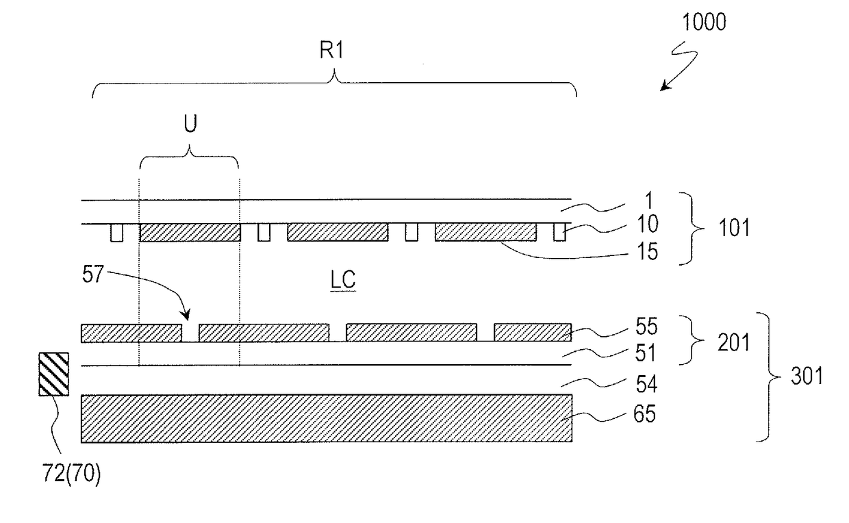
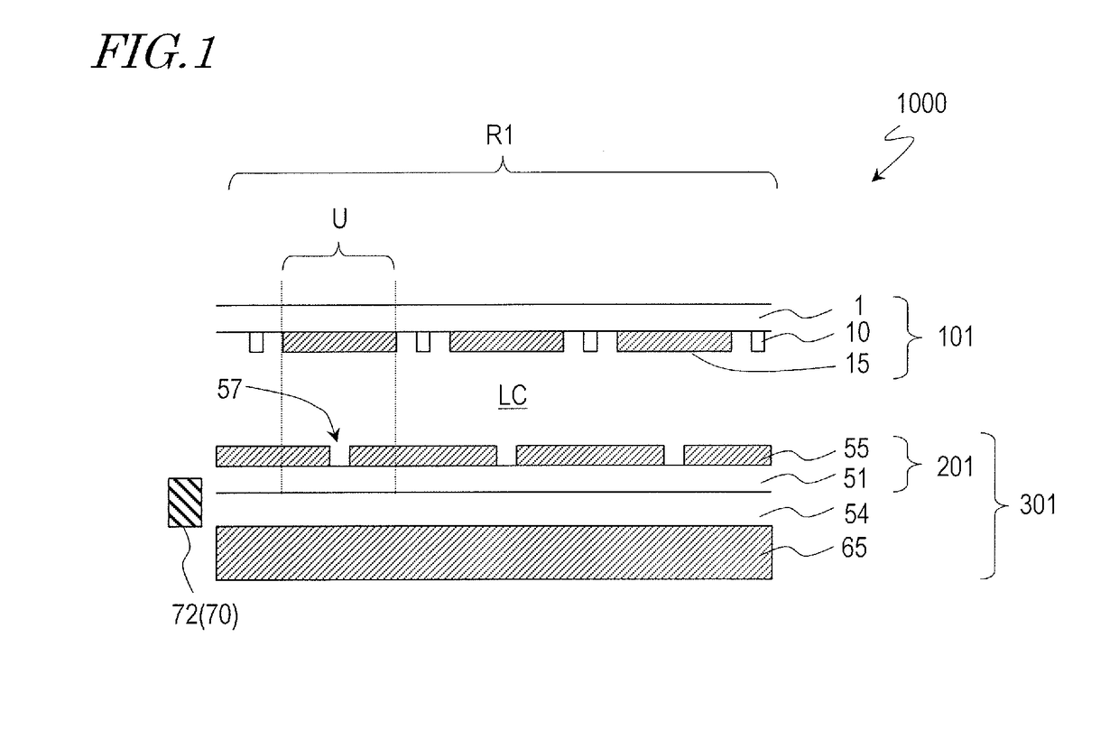
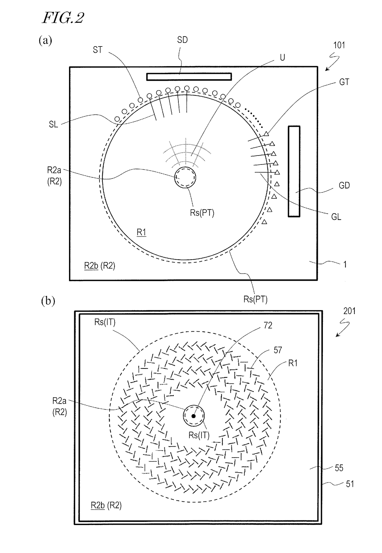
[0110]First, reference will be made to FIG. 1 and FIG. 2. FIG. 1 is a schematic partial cross-sectional view at around the center of the scanned antenna 1000 as described in detail above, and FIGS. 2(a) and 2(b) are schematic plan views showing the TFT substrate 101 and the slot substrate 201, respectively, of the scanned antenna 1000.

[0111]The scanned antenna 1000 includes a plurality of antenna elements U arranged in a two-dimensional arrangement, and the scanned antenna 1000 illustrated herein includes a plurality of antenna elements arranged in a concentric arrangement. In the following description, the region of the TFT substrate 101 or the slot substrate 201 corresponding to the antenna element U will be referred to as an “antenna element region” and will be denoted by the same reference sign U as the antenna element. As shown in FIGS. 2(a) and 2(b), in the TFT substrate 101 and the slot substrate 201, a region defined by a plurality of antenna element regions arranged in a tw...

second embodiment

[0203]A scanned antenna according to a second embodiment will be described with reference to the drawings. The TFT substrate of the scanned antenna of the present embodiment is different from the TFT substrate 101 shown in FIG. 2 in that the transparent conductive layer to be the upper connecting portions of the terminal portions is provided between the first insulating layer and the second insulating layer of the TFT substrate.

[0204]FIG. 8(a) to (c) are cross-sectional views showing the gate terminal portion GT, the source terminal portion ST and the transfer terminal portion PT, respectively, of the TFT substrate 102 of the present embodiment. Like elements to those of FIG. 4 are denoted by like reference signs and will not be discussed below. Note that the cross-sectional structure of the antenna element region U will not be shown in the figures or discussed below as it is similar to that of the embodiment described above (FIG. 3).

[0205]The gate terminal portion GT of the present...

third embodiment

[0220]A scanned antenna according to a third embodiment will be described with reference to the drawings. The TFT substrate of the scanned antenna of the present embodiment is different from the TFT substrate 102 shown in FIG. 8 in that the upper connecting portion formed from a transparent conductive film is absent in the transfer terminal portion.

[0221]FIG. 10(a) to (c) are cross-sectional views showing the gate terminal portion GT, the source terminal portion ST and the transfer terminal portion PT, respectively, of the TFT substrate 103 of the present embodiment. Like elements to those of FIG. 8 are denoted by like reference signs and will not be discussed below. Note that the structure of the antenna element region U will not be shown in the figures or discussed below as it is similar to that of the embodiment described above (FIG. 3).

[0222]The structure of the gate terminal portion GT and the source terminal portion ST is similar to the structure of the gate terminal portion a...


PUM


Abstract

A scanned antenna (1000) is a scanned antenna including antenna elements (U) arranged together, the scanned antenna including: a TFT substrate (101) including a first dielectric substrate (1), TFTs, gate bus lines, source bus lines, and patch electrodes (15); a slot substrate (201) including a second dielectric substrate (51) a slot electrode (55); a liquid crystal layer (LC) provided between the TFT substrate and the slot substrate; and a reflective conductive plate (65). The slot electrode includes slots (57) arranged so as to correspond to the patch electrodes. As seen from the normal direction to the first dielectric substrate, a plurality of spacer structures (75) provided between the TFT substrate and the slot substrate are arranged so as not to overlap with first regions (Rp1) and/or second regions (Rp2), where the first regions are regions that are within a distance of 0.3 mm from edges of the slots and the second regions are regions that are within a distance of 0.3 mm from edges of the patch electrodes.

Description

TECHNICAL FIELD[0001]The present invention relates to a scanned antenna, and particularly to a scanned antenna (which may be referred to as a “liquid crystal array antenna”) in which each antenna element (which may be referred to as an “element antenna”) includes a liquid crystal capacitor.BACKGROUND ART[0002]Antennas for mobile communication and satellite broadcasting applications need to have the capability of changing the beam direction (referred to as “beam scanning” or “beam steering”). As antennas having such a capability (hereinafter referred to as “scanned antennas”), phased array antennas including antenna elements have been known in the art. However, the high cost of conventional phased array antennas has been an obstacle for their widespread application to consumer products. Particularly, the cost increases significantly when the number of antenna elements increases.[0003]In view of this, scanned antennas have been proposed in the art that utilize the high dielectric anis...

Claims


Application Information

Patent Timeline
IPC IPC(8): H01Q3/44H01Q13/10H01L27/12H01L23/66
CPCH01Q3/44H01Q13/10H01L27/124H01L23/66H01L27/1262H01L27/1218H01L2223/6677H01L29/78669H01L29/78678H01L29/7869H01L29/66969H01L29/66765H01Q3/34H01Q13/22H01Q21/06H01Q1/364G02F1/1313G02F1/1362G02F1/136213G02F2202/42G02F2203/62H01L27/1225G02F1/292G02F1/13394H01Q1/125H01Q1/243H01Q3/46H01Q3/242
Inventor NAKAZAWA, MAKOTOORUI, TAKATOSHINAKAMURA, WATARUOHTAKE, TADASHINAKANO, FUMIKIMINOURA, KIYOSHI
Owner SHARP KK
Why Eureka
Try Eureka