Semiconductor templates and fabrication methods

a technology of semiconductors and templates, applied in the field of semiconductor templates and methods, to achieve the effect of preventing the growth of semiconductor materials

Inactive Publication Date: 2018-06-14
SEREN PHOTONICS
View PDF2 Cites 2 Cited by
  • Summary
  • Abstract
  • Description
  • Claims
  • Application Information

AI Technical Summary

Benefits of technology

[0010]Each of the columns may have a cap on its top during growth of the semiconductor material. The cap may comprise at least one mask layer or part of a mask layer. The cap may be arranged to prevent growth of the semiconductor material from the top of the column. The height of the cap may be at least high enough so that the propagation of BSFs from the highest point

Problems solved by technology

However it can be a problem with this method that a considerable fraction of basal stacking faults in the crystal structure of

Method used


Image

  • Semiconductor templates and fabrication methods
  • Semiconductor templates and fabrication methods
  • Semiconductor templates and fabrication methods

Examples


Embodiment Construction

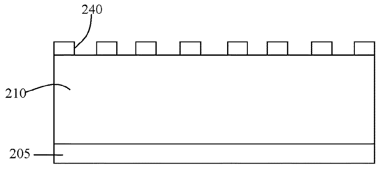
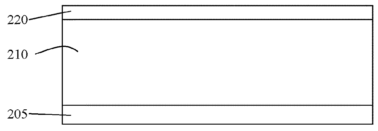
[0049]Referring to FIG. 1a, the first step of fabricating a semiconductor template is providing a suitable semiconductor wafer 201. The wafer 201 is conventional and is made up of a substrate 205, which in this case comprises a layer of sapphire, over which is a semiconductor layer 210 formed of gallium nitride (GaN). Other materials can be used. For example the substrate may be silicon (either planar or patterned) or silicon carbide (either planar or patterned). The semiconductor may be another suitable material, for example another group III nitride such as indium gallium nitride (InGaN) or aluminium gallium nitride (AlGaN) or indium nitride (InN) or aluminium nitride (AlN). The semiconductor wafer is semipolar. Specifically in this embodiment the GaN is orientated so that its top surface, parallel to the plane of the substrate, which is referred to herein as the horizontal plane, is in the (11-22) plane. A buffer layer or nucleation layer, for example of high temperature MN with ...


PUM


Abstract

A method of making a semi-polar semiconductor template comprises providing a semi-polar semiconductor wafer; etching the semiconductor wafer to form a regular semiconductor structure comprising a plurality of semiconductor regions (260) with a plurality of gaps between the regions, each of the regions (260) having a sidewall facing a respective one of the gaps, and growing semiconductor material over the semiconductor structure. The semiconductor material has a preferential growth direction (c) in which growth proceeds most rapidly from each of the sidewalls, and each of the sidewalls has at least a part which faces a vertical centre line of the respective one of the gaps so that growth in the preferential direction from said part extends towards said vertical centre line.

Description

FIELD OF THE INVENTION[0001]The invention relates to semiconductor templates and methods of making semiconductor templates. In particular the invention relates to the production of semiconductor templates with high quality crystal structure. The templates can be used, for example, in the formation of light emitting diodes and solid state lasers.BACKGROUND TO THE INVENTION[0002]Our earlier patent application PCT / GB2012 / 050458 describes a method of growing semiconductor crystal structures, for example GaN crystal structures, in which an irregular array of columns, also referred to as nano-columns, micro-columns, rods or pillars, is formed, and then a layer of semiconductor material is grown laterally from the sides of the columns and then over the tops of the columns, with a mask layer on the tops of the columns preventing growth from the tops of the columns, which helps to prevent the propagation of threading, edge, and mixed dislocations upwards from the tops of the columns. However...

Claims


Application Information

Patent Timeline
IPC IPC(8): H01L21/02
CPCH01L21/02458H01L21/02516H01L21/0254H01L21/0265H01L21/02609H01L21/02603
Inventor WANG, TAO
Owner SEREN PHOTONICS
Why Eureka
Try Eureka