Ternary puf unit and circuit realized by cnfet

a field effect transistor and puf technology, applied in the field of physical unclonable function units, can solve the problems of gate time delay and interconnect crosstalk brought forth by parasitic effect of interconnecting lines, increase the number of challenge-response pairs, and achieve better randomness and uniqueness, and the effect of high randomness and uniqueness

Inactive Publication Date: 2018-06-14
NINGBO UNIV
View PDF0 Cites 5 Cited by
  • Summary
  • Abstract
  • Description
  • Claims
  • Application Information

AI Technical Summary

Benefits of technology

[0011]As compared with prior arts, the ternary PUF circuit according to the present invention has the following advantage: the ternary PUF units in the ternary PUF unit array form a cross-coupling inverter via the 2nd CNFET transistor, the 3rd CNFET transistor, the 4th CNFET transistor, the 5th CNFET transistor, the 6th CNFET transistor and the 7th CNFET transistor; the variations current is incurred by the cross-coupling inverter due to process variations; the random and unclonable ternary output signals “0”, “1” and “2” are obtained through current competition of the ternary PUF unit; HSPICE in the 32 nm CNFET standard model base is used for Monte Carlo simulation of the ternary PUF circuit according to the present invention for analysis of its performance as randomness and uniqueness; as indicated by simulation results, randomness of the ternary PUF circuit according to the present invention is 33.21%, which is extremely approximate to the ideal value of 33.33%; whereas, uniqueness is 66.75%, which is almost equal to the ideal value of 66.66%; therefore, it is provided with higher randomness and uniqueness; smaller area of circuit can ensure better randomness and uniqueness on condition that correct logic function can be maintained.

Problems solved by technology

The attacker is unable to clone the PUF circuit with identical output response due to uncontrollable process variations despite of the fact that the attacker knows structure of the PUF circuit.
PUF circuit can defense numerous conventional attacks owing to its unclonable properties.
In the silicon PUF circuit, such problems as gate time delay and interconnect crosstalk brought forth by parasitic effect of interconnecting line will become more and more serious once the characteristic dimension is reduced to the nanometer scale.
For binary PUF circuit, increased quantity of challenge-response pairs will inevitably increase the area of chips.

Method used


Image

  • Ternary puf unit and circuit realized by cnfet
  • Ternary puf unit and circuit realized by cnfet
  • Ternary puf unit and circuit realized by cnfet

Examples


Embodiment Construction

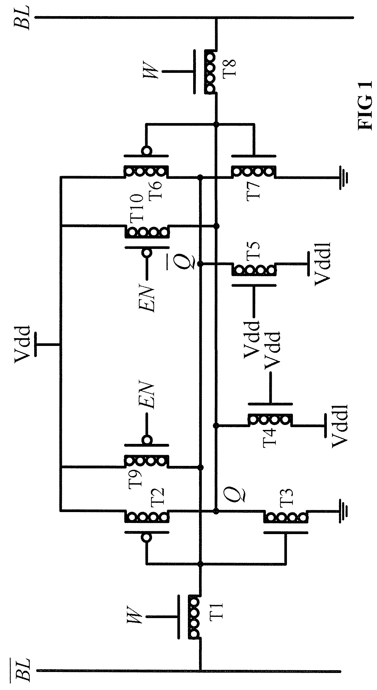
[0019]The present invention discloses a ternary PUF unit realized by CNFET; the ternary PUF unit realized by CNFET according to the present invention is further described as follows in combination with embodiments to drawings.

[0020]Embodiment: A ternary PUF unit realized by CNFET as shown in FIG. 1 comprising the 1st CNFET transistor T1, the 2nd CNFET transistor T2, the 3rd CNFET transistor T3, the 4th CNFET transistor T4, the 5th CNFET transistor T5, the 6th CNFET transistor T6, the 7th CNFET transistor T7, the 8th CNFET transistor T8, the 9th CNFET transistor T9 and the 10th CNFET transistor T10; the 1st CNFET transistor T1, the 3rd CNFET transistor T3, the 4th CNFET transistor T4, the 5th CNFET transistor T5, the 7th CNFET transistor T7 and the 8th CNFET transistor T8 belong to N CNFET transistors; the 2nd CNFET transistor T2, the 6th CNFET transistor T6, the 9th CNFET transistor T9 and the 10th CNFET transistor T10 belong to P CNFET transistors; gate of the 1st CNFET transistor ...


PUM


Abstract

The present invention discloses a ternary PUF unit and circuit realized by CNFET; the ternary PUF circuit comprises a ternary row decoder, a ternary column decoder, a ternary output circuit and a ternary PUF unit array; the said ternary PUF circuit is arranged into a 3n rows×3n columns matrix formed by 3n×3n ternary PUF units; the ternary PUF unit comprises a 1st CNFET transistor, a 2nd CNFET transistor, a 3rd CNFET transistor, a 4th CNFET transistor, a 5th CNFET transistor, a 6th CNFET transistor, a 7th CNFET transistor, an 8th CNFET transistor, a 9th CNFET transistor and a 10th CNFET transistor; its advantage lies in the fact that it is provided with small circuit area and higher randomness and uniqueness while ensuring proper logic function.

Description

CROSS-REFERENCE TO RELATED APPLICATION[0001]This application claims the priority benefit of China application no. 201611119524.8, filed on Dec. 8, 2016. The entirety of the abovementioned patent application is hereby incorporated by reference herein and made a part of this specification.FIELD OF THE INVENTION[0002]The present invention is related a Physical Unclonable Function (PUF) unit, in particular to a ternary PUF unit and circuit realized by Carbon Nanotube Field Effect Transistor (CNFET).BACKGROUND ART[0003]Physical Unclonable Function (PUF) makes use of random process variations during manufacturing of integrated circuit to produce cipher for application to the password system. Due to random process variations, different chips of the same structure may obtain different output responses under the same excitation. The attacker is unable to clone the PUF circuit with identical output response due to uncontrollable process variations despite of the fact that the attacker knows s...

Claims


Application Information

Patent Timeline
Patent Type & Authority Applications(United States)
IPC IPC(8): H01L23/00H01L27/28H04L9/32
CPCH01L23/576H04L9/3278H01L27/283G09C1/00H10K19/10
Inventor WANG, PENGJUNGONG, DAOHUIZHANG, HUIHONGKANG, YAOPENG
Owner NINGBO UNIV
Why Eureka
Try Eureka