Method for making a semiconductor device with self-aligned inner spacers

a technology of inner spacers and semiconductors, applied in the field of making a semiconductor device, can solve the problems of difficult alignment between the inner edges of the outer spacers and the side the difficulty of aligning between the channel region and the walls of the cavities,

Active Publication Date: 2018-06-21
COMMISSARIAT A LENERGIE ATOMIQUE ET AUX ENERGIES ALTERNATIVES
View PDF0 Cites 56 Cited by
  • Summary
  • Abstract
  • Description
  • Claims
  • Application Information

AI Technical Summary

Benefits of technology

[0048]Thus, the difference in oxidation rate between the semiconductor of the first portion and that of the second portions may be advantageously achieved thanks to the difference

Problems solved by technology

The method described in this document however raises a problem.
Indeed, given that the cavity (cavities) formed within the stack for making inner spacers is (are) obtained by etching without a barrier layer, the alignment attempted between the inner edges of the outer spacers and the side walls of the cavities

Method used


Image

  • Method for making a semiconductor device with self-aligned inner spacers
  • Method for making a semiconductor device with self-aligned inner spacers
  • Method for making a semiconductor device with self-aligned inner spacers

Examples


first embodiment

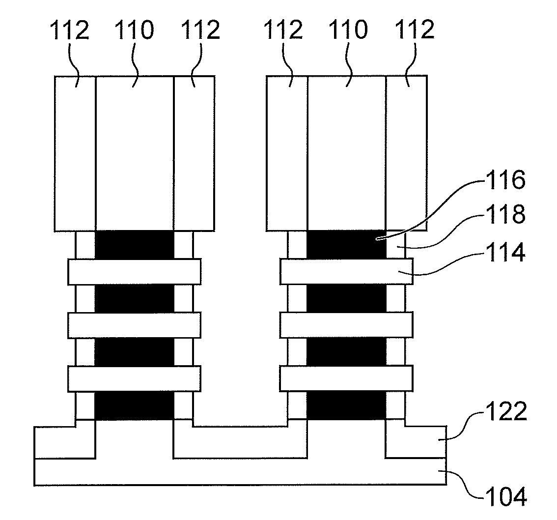
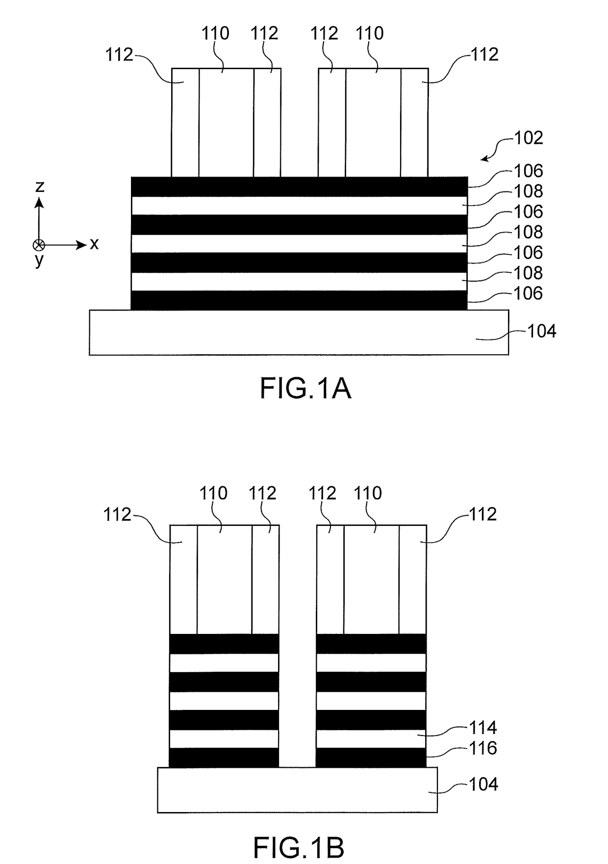
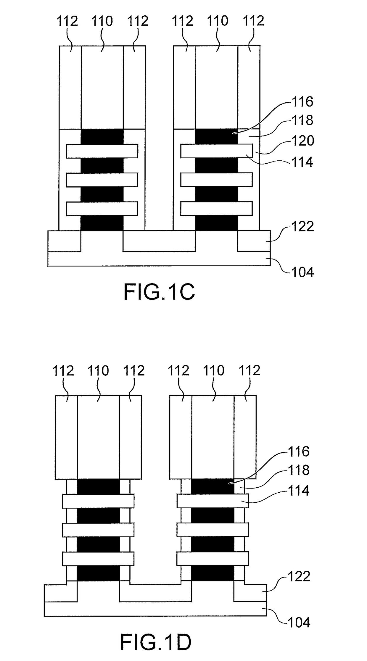
[0059]FIGS. 1A to 1G are first referred to which show the steps of a method for making a semiconductor device 100 including herein two P-type GAA-FET transistors, according to a

[0060]As shown in FIG. 1A, the device 100 is made from a stack 102 of layers of different materials which is arranged on a substrate 104. In the first embodiment described here, the substrate 104 corresponds to a “bulk” semiconductor substrate, for example of silicon or SiGe. The stack 102 comprises layers 106, 108 of two different materials and alternately arranged above each other. Each of the layers 108 is intended to form one or more semiconductor nanowires of one or more channels of the device 100 and is arranged between two layers 106 including a material able to be selectively etched relative to that of the layers 108. In the first embodiment described herein, the stack 102 includes three layers 108 as well as four layers 106 alternately arranged such that each of the layers 108 is arranged between two...

second embodiment

[0096]A method for making the device 100 is described in connection with FIGS. 2A to 2D.

[0097]The initial stack 102 used in this second embodiment is similar to that used in the first embodiment.

[0098]The steps previously described in connection with FIGS. 1A and 1B are first implemented. However, unlike the first embodiment in which the nanowires 114 are broken between two transistors, the etching of the stack 102 which is implemented is such that the nanowires 114 of the two transistors are here formed by continuous portions which are not broken at the future common source and drain region intended to be made for both these transistors. The structure obtained is shown in FIG. 2A.

[0099]As for the first embodiment previously described, a partial oxidation of the portions 116, from the surfaces forming the side flanks of the structures obtained by implementing the previous etching, is then implemented, forming the inner spacers 118.

[0100]Further, a part of the nanowires 114 is oxidi...

third embodiment

[0112]A method for making the device 100 is described in connection with FIGS. 3A to 3I. In these Figs., making a single GAA-FET transistor is described.

[0113]The initial stack 102 used in this third embodiment is similar to that used in the first and second embodiments.

[0114]As in the first and second embodiments previously described, the stack 102 is first etched as one or more elongate portions (a single elongate portion being shown in FIG. 3A), and then a dummy gate 110 and temporary outer spacers 301 are then made on the elongate portion formed from the stack 102, without a subsequent etching of the parts of the stack 102 which are not covered with the temporary outer spacers 301.

[0115]A packaging material 303 is then deposited onto the parts of the layers 106, 108 at which the future source and drain regions of the transistor will be made (FIG. 3A).

[0116]As shown in FIG. 3B, the temporary outer spacers 301 as well as the parts of the layers 106, 108 which are covered with the...


PUM


Abstract

A method for making a semiconductor device, including:
    • a) making, on a substrate, a stack comprising a first semiconductor portion able to form an active zone and arranged between two second portions of a material able to be selectively etched relative to the semiconductor of the first portion,
    • b) making, on a part of the stack, outer spacers and a dummy gate,
    • c) etching the second portions such that remaining parts are arranged under the dummy gate,
    • d) partially oxidising the remaining parts from the outer faces, forming inner spacers,
    • e) removing the dummy gate and non-oxidised parts of the remaining parts arranged under the dummy gate,
    • f) making a gate between the outer spacers and between the inner spacers and covering the channel.

Description

TECHNICAL FIELD AND PRIOR ART[0001]The invention relates to a method for making a semiconductor device comprising one or more transistors, for example of the GAA-FET (“Gate-All-Around Field Effect Transistor”) type, and inner spacers being self-aligned with respect to each other.[0002]In a GAA-FET-type transistor, the gate of the transistor is made all around the channel such that the channel is surrounded or encapsulated by the gate. Such a transistor has the advantage, in comparison with a conventional MOSFET transistor, of improving the electrostatic control of the channel by the gate (which enables the leakage currents to be reduced), in particular when the transistor is fully depleted (for example of the FD-SOI, or Fully-Depleted Silicon On Insulator, type).[0003]It is known to make a GAA-FET-type transistor comprising a stack of several semiconductor nanowires forming the channel of the transistor together. This configuration makes it possible to achieve a good compromise betw...

Claims


Application Information

Patent Timeline
IPC IPC(8): H01L29/66H01L29/06H01L29/423H01L29/78H01L21/02
CPCH01L29/66553H01L29/6681H01L29/0673H01L29/42392H01L29/7853H01L29/66818H01L29/6656H01L21/02236H01L21/02238H01L21/02255H01L29/6653H01L29/78696B82Y10/00H01L21/823807H01L21/823814H01L21/823864H01L29/41725H01L29/66439H01L29/775H01L27/092H01L29/0653H01L29/7848
Inventor REBOH, SHAYAUGENDRE, EMMANUELCOQUAND, REMI
Owner COMMISSARIAT A LENERGIE ATOMIQUE ET AUX ENERGIES ALTERNATIVES
Why Eureka
Try Eureka