Photon detection device and photon detection method

Active Publication Date: 2018-07-05
NAT INST OF ADVANCED IND SCI & TECH
View PDF3 Cites 4 Cited by
  • Summary
  • Abstract
  • Description
  • Claims
  • Application Information

AI Technical Summary

Benefits of technology

[0013]An object of the present invention is to provide a photon detection device and a photon detection method, which solve the aforementioned various problems in the conventional techn

Problems solved by technology

However, the current safety key generation rate is not sufficient and not practical.
Conventionally, an InGaAs avalanche photodiode (APD) has been widely used for photon detection in the communication wavelength band (1,550 nm), but there are problems of afterpulse generation and a large dark count.
These problems are factors in increase of an error rate of key generation, but it is difficult to

Method used


Image

  • Photon detection device and photon detection method
  • Photon detection device and photon detection method
  • Photon detection device and photon detection method

Examples


first embodiment

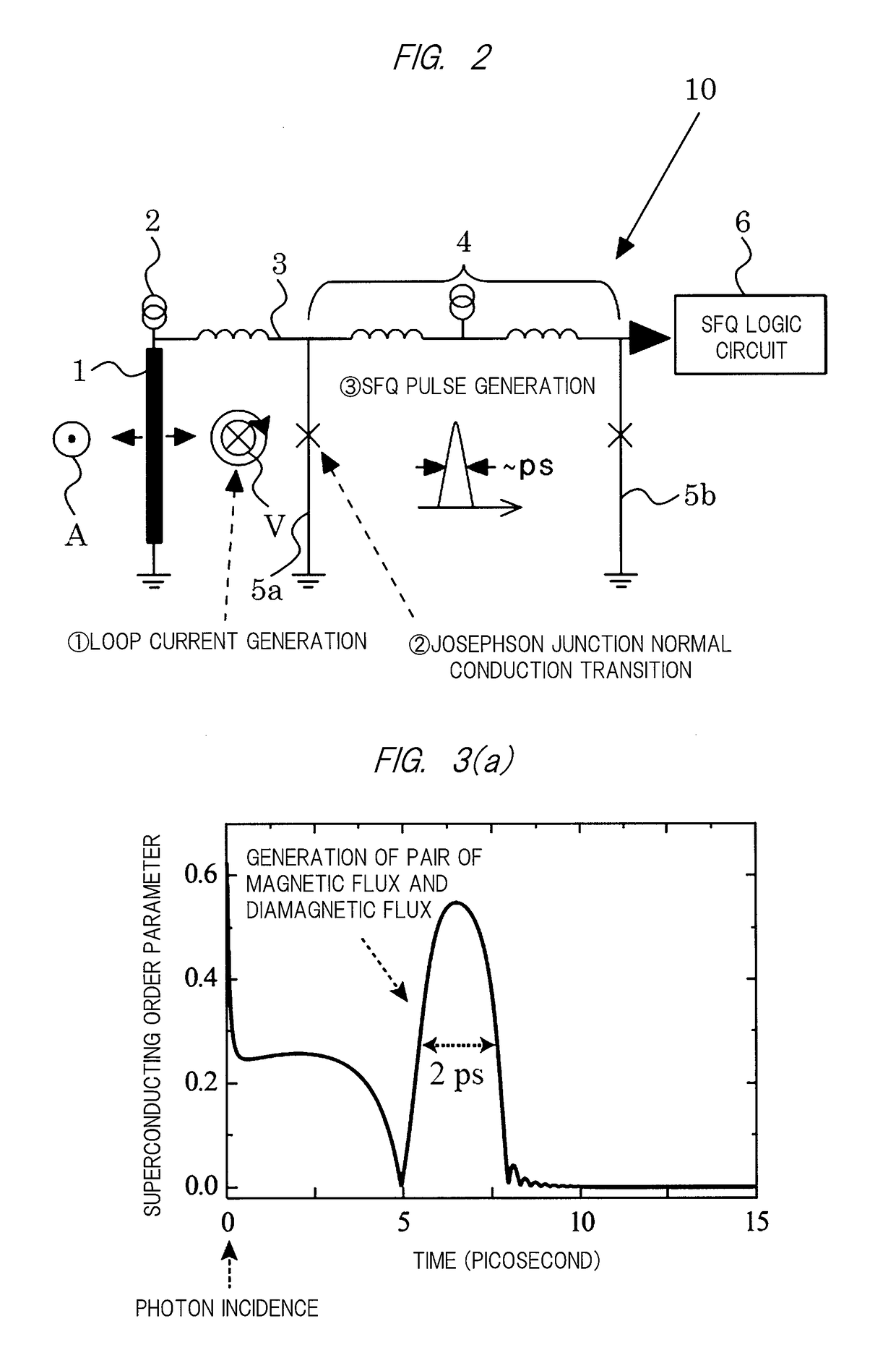
[0042]An outline of a first embodiment of the present invention is illustrated in FIG. 2.

[0043]A photon detection device 10 mainly includes a superconducting stripline 1 and a Josephson transmission line (JTL) circuit 4 serving as a single flux quantum (SFQ) circuit.

[0044]The superconducting stripline 1 is a long plate-shaped member whose plate surface is a photon detection surface. This superconducting stripline 1 is not particularly limited and may be suitably selected from known ones to be used.

[0045]Moreover, a shape of the superconducting stripline 1 is not particularly limited. Herein, the superconducting stripline 1 has a linear shape for the purpose of stabilizing magnetic flux detection in the JTL circuit 4 by excluding the magnetic flux, which is excluded from the superconducting stripline 1, in a direction orthogonal to a length direction of the line. However, even in the case of the linear shape, this does not hinder addition of a portion with a shape other than a linear...

second embodiment

[0080]Next, a second embodiment of the present invention will be described. FIG. 4 is an explanatory diagram illustrating an outline of the second embodiment of the present invention.

[0081]A photon detection device 50 is mainly constituted by monolithically forming superconducting striplines 1a to 1d, JTL circuits 4a to 4d, integrated input circuits (confluence buffer (CB)) 7a to 7c, an SFQ logic circuit 6, an optical waveguide 8b, photon detection sections, and a comparator circuit on a substrate 8a. Note that, since the detail of each part of the superconducting striplines 1a to 1d, the JTL circuits 4a to 4d, the SFQ logic circuit 6, the photon detection sections, and the comparator circuit is the same as that of each of the superconducting stripline 1, the JTL circuit 4, the SFQ logic circuit 6, the photon detection section, and the comparator circuit in the photon detection device 10, descriptions on configuration and operation of each part are omitted.

[0082]The superconducting ...

third embodiment

[0093]Next, a third embodiment of the present invention will be described. FIG. 5 is an explanatory diagram illustrating an outline of the third embodiment of the present invention.

[0094]A photon detection device 100 illustrated in FIG. 5 is constituted as a monolithic device in which a plurality of photon detection arrays 9 in the photon detection device 50 illustrated in FIG. 4 are arranged on the same substrate. Other than this, the photon detection device 100 is the same as the photon detection device 50, and thus, description thereof is omitted.

[0095]According to this photon detection device 100, a photon from a light supply source such as an independent optical fiber or the like can be independently detected by each photon detection array 9, and communication signals from a plurality of information sources can be processed. For example, in a setup of polarization (4)×dual wavelength multiplexing (2)×transmission / reception (2), which is the basic setup of quantum entangled quan...


PUM


Abstract

Provided are a photon detection device and a photon detection method being practical, capable of performing photon detection in which no afterpulse is generated and generation of a dark count is suppressed, and capable of obtaining a high counting rate with low jitter. The photon detection device of the present invention includes: a photon detection section having a long plate-shaped superconducting stripline whose plate surface is a photon detection surface, and a bias current supply section supplying a bias current to the superconducting stripline; and a single flux quantum comparator circuit capable of detecting magnetic flux scattered from the superconducting stripline upon photon detection.

Description

CROSS-REFERENCE TO RELATED APPLICATIONS[0001]This application is a National Stage application of International Patent Application No. PCT / JP2016 / 067747, filed on Jun. 15, 2016, which claims priority to Japanese Patent Application Number 2015-123764, filed on Jun. 19, 2015, each of which is hereby incorporated by reference in its entirety.TECHNICAL FIELD[0002]The present invention relates to a photon detection device and a photon detection method using a superconducting stripline.BACKGROUND ART[0003]Securing information safety is an urgent task of the network society, and quantum cryptographic communication is expected as a core technology.[0004]However, the current safety key generation rate is not sufficient and not practical. To realize a practical safety key generation rate, it is essential to achieve higher performance of a photon detector, which is an urgent task.[0005]Conventionally, an InGaAs avalanche photodiode (APD) has been widely used for photon detection in the communic...

Claims


Application Information

Patent Timeline
IPC IPC(8): G01J1/44G01J1/02H01L39/10H01L39/02
CPCG01J1/44G01J1/02H01L39/10H01L39/025H04L9/0852G01J2001/442G01J2001/4446H10N60/00H10N60/10H10N60/84H10N60/805
Inventor ZEN, NOBUYUKIMAWATARI, YASUNORIFUJII, GOYOSHIKAWA, NOBUYUKI
Owner NAT INST OF ADVANCED IND SCI & TECH
Why Eureka
Try Eureka