Highly Tunable, Low Jitter Optical Clock Generation

Inactive Publication Date: 2010-09-16
FTL SYST
View PDF12 Cites 4 Cited by
  • Summary
  • Abstract
  • Description
  • Claims
  • Application Information

AI Technical Summary

Benefits of technology

[0007]The present invention consists of (1) a source of continuous wave laser emissions with narrow optical bandwidth [FIG. 1; Block 1] (2) a means of optically splitting the laser emission into a carrier and one or more beams to be modulated [FIG. 1; Block 2] (3) one or more digitally controlled time-lens capable of dividing the laser emission frequency down to a modulation frequency [FIG. 1; Block 3] (4) one or more optically controlled, optical modulators [FIG. 1; Block 4]. In order to facilitate planar, monolithic implementations of the time-lens [3] and m

Problems solved by technology

Variations in the periodicity of waveforms, known as jitter, reduce the efficiency of systems using the timing or communications signal.
In order to accommodate such a range, less work is typically done during each period by components utilizing the clock signal, usually resulting in a less efficient system.
In order to accommodate variations in the periodicity of a communications signal the period must typically be lengthened, thus reducing the data transfer rate, usually resulting in a less efficient transmission system.
As the carrier and modulation frequency approach each other or the carrier and modulation amplitude approach each other the resulting jitter will increase.
This is known as time-varying skew and can decrease system efficiency.
At the point of use, optical clock signals may be converted into electronic signals where required, although with increased jitter and skew.
As clocks increase in frequency from tens of MegaHertz into the TeraHertz range, tuning ranges typically become more restricted, resulting in a more limited range of periods which can be externally controlled.
Such limitations in the clock period which can be attained through tuning limit the utility of a clock system.

Method used


Image

  • Highly Tunable, Low Jitter Optical Clock Generation
  • Highly Tunable, Low Jitter Optical Clock Generation
  • Highly Tunable, Low Jitter Optical Clock Generation

Examples


Embodiment Construction

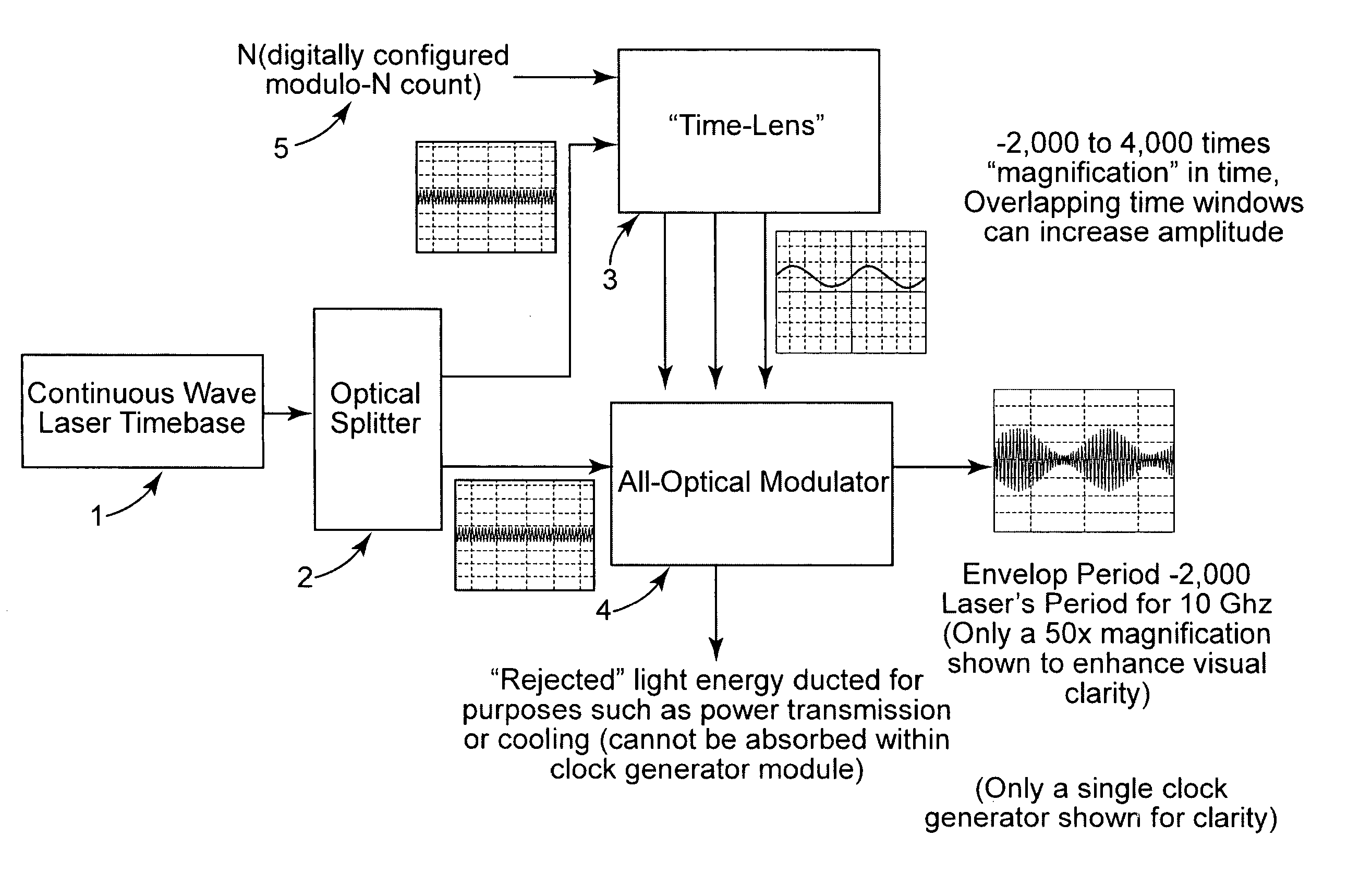
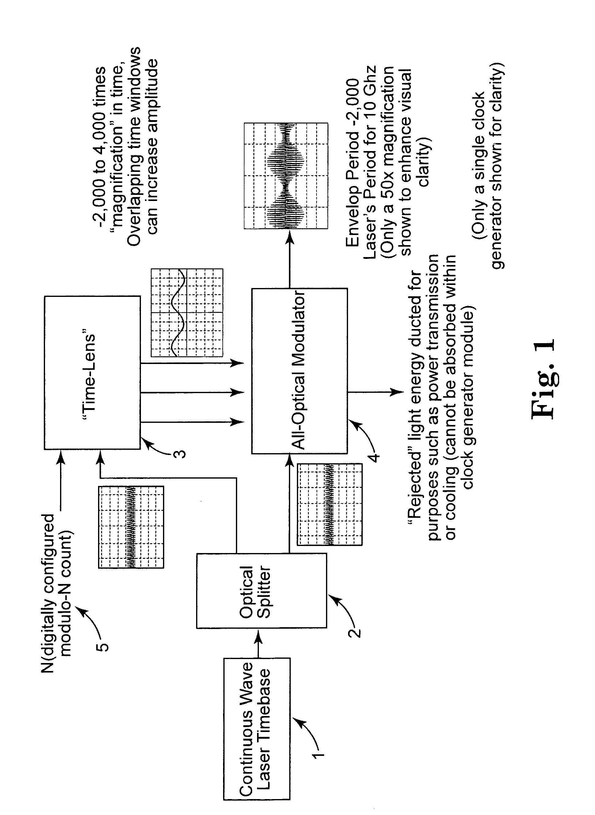
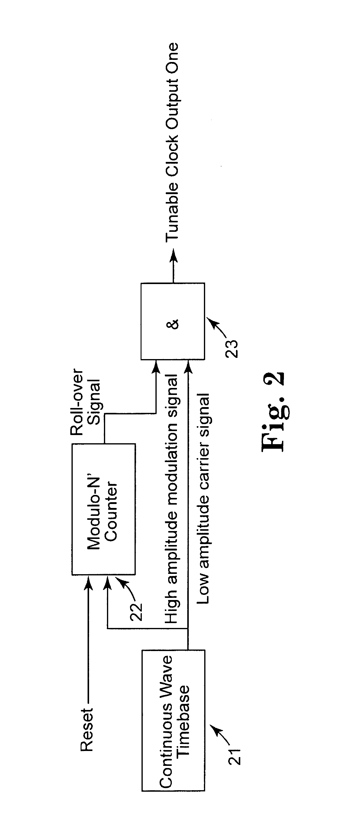
[0015]The optical embodiment of the invention may be most rapidly understood by starting with an abstract digital model of the invention (FIG. 2). A continuous wave timebase [Block 21] drives a logical AND (denoted per IEEE standards with &) gate [Block 23] both directly and through a modulo-N counter [Block 22]. The resulting clock output has a period which is 2*N times the period of the continuous wave time base.

[0016]The AND gate in this model [Block 23] is not actually a boolean AND gate. When the modulation signal is logic low, the low amplitude carrier signal passes through the AND gate at a low amplitude. When the modulation signal from the Modulo-N counter is high (second half of the count range), the carrier signal is greatly amplified but retains the same carrier frequency. When the clock signal is received, the carrier frequency must be “averaged out”, yielding a conventional square wave clock at an output frequency much lower than the carrier frequency. Transmitting such...


PUM


Abstract

An apparatus is disclosed for the optical generation of clock signals with tunable frequency and low jitter. A laser source serves as both the carrier used to transmit the clock signal for use by other optical, electronic or hybrid circuit elements and the original modulation time base. A fraction of the original laser source undergoes one or more stages of frequency division before being recombined as a modulation signal with the remaining laser beam. Transmission of the resulting signal via single mode fiber and dividers retains the low jitter properties of the modulated signal. By starting with a clock signal of optical frequency then dividing downward in frequency, comparatively high frequency clocks may be generated, notably in the GigaHertz and TeraHertz frequency ranges.

Description

FIELD OF THE INVENTION[0001]Clock circuits supply a periodic waveform. The periodic waveform usually approximates a square wave, trapezoidal wave or sine wave resulting from frequency limitations of the generation and transmission circuit. In many electronic and optical generation and transmission systems, the periodic waveform amplitude-modulates a much higher frequency periodic waveform known as the carrier. For example, an optical carrier with a 1510 nm wavelength or approximately 200 TeraHertz may be amplitude-modulated by a periodic waveform at 10 GigaHertz. Simple periodic waveforms communicate a timing signal used to synchronize a multiplicity of receiving circuits, as in a computer system. More complex periodic waveforms may encode information to provide data communication on one or more channels. Examples of such information include voice, video or computer files communicated from one location to another.[0002]Variations in the periodicity of waveforms, known as jitter, red...

Claims


Application Information

Patent Timeline
IPC IPC(8): H04B10/06
CPCH04L7/0008H04B10/50
Inventor WILLIS, JOHN C.BETCHER, RUTH A.
Owner FTL SYST
Why Eureka
Try Eureka