
Clock/data recovery circuit

Inactive Publication Date: 2006-08-22
NIPPON TELEGRAPH & TELEPHONE CORP
View PDF14 Cites 12 Cited by
  • Summary
  • Abstract
  • Description
  • Claims
  • Application Information

AI Technical Summary

Benefits of technology

[0103]In addition, according to the present invention, a receiving apparatus including the clock / data recovery circuit can be provided. The receiving apparatus can be applied to an optical front end circuit receiver and the like in a router or in a cross connect part in SDH / SONET, point to point transmission, GbE / 10GbE and Fiber Channel in an optical communication system. According to the receiving apparatus, the low jitter, small size and low power consumption can be realized. As a result, lowering cost of an optical front end module can be realized and the cost of a communication system can be decreased.

Problems solved by technology

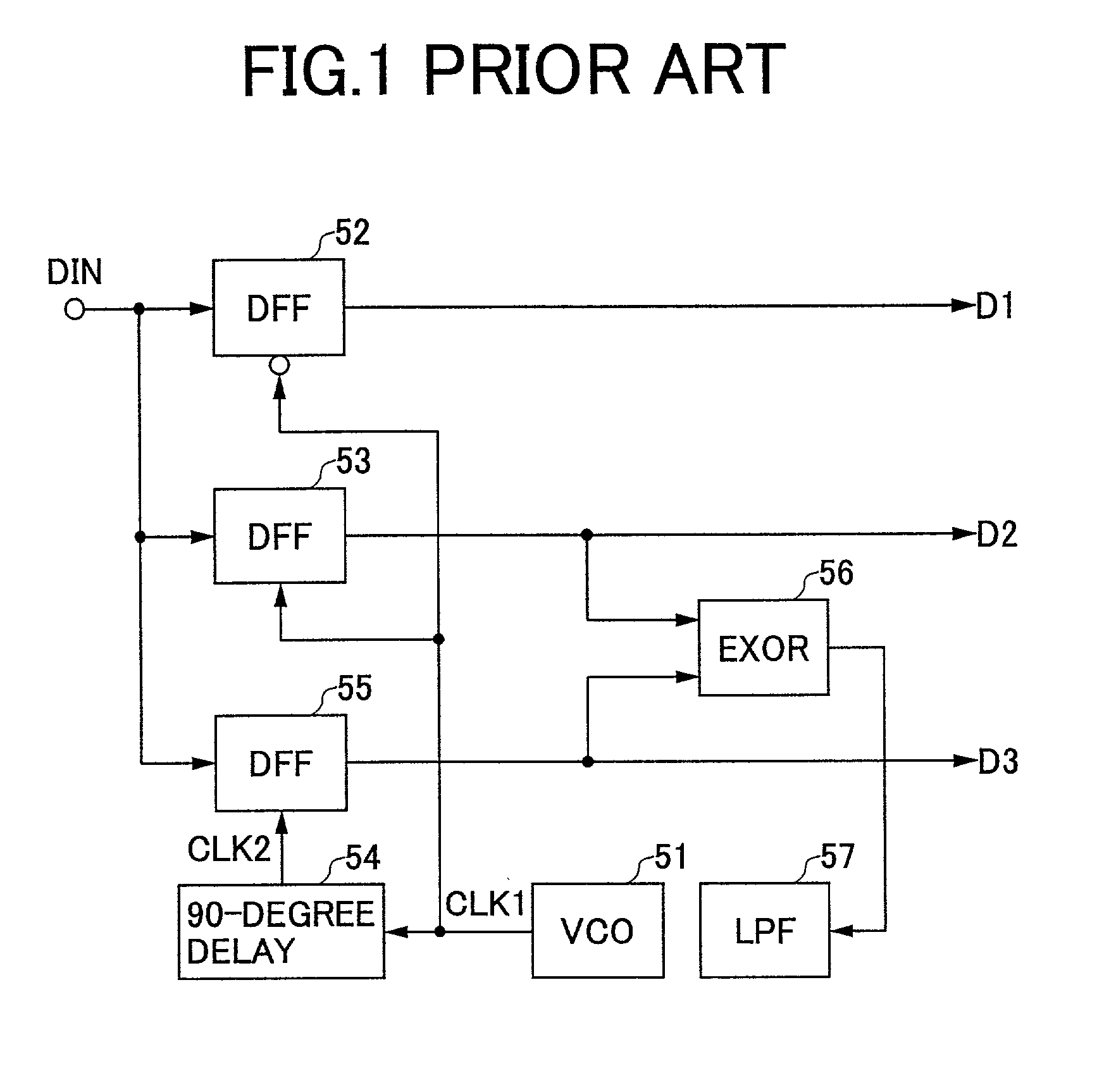
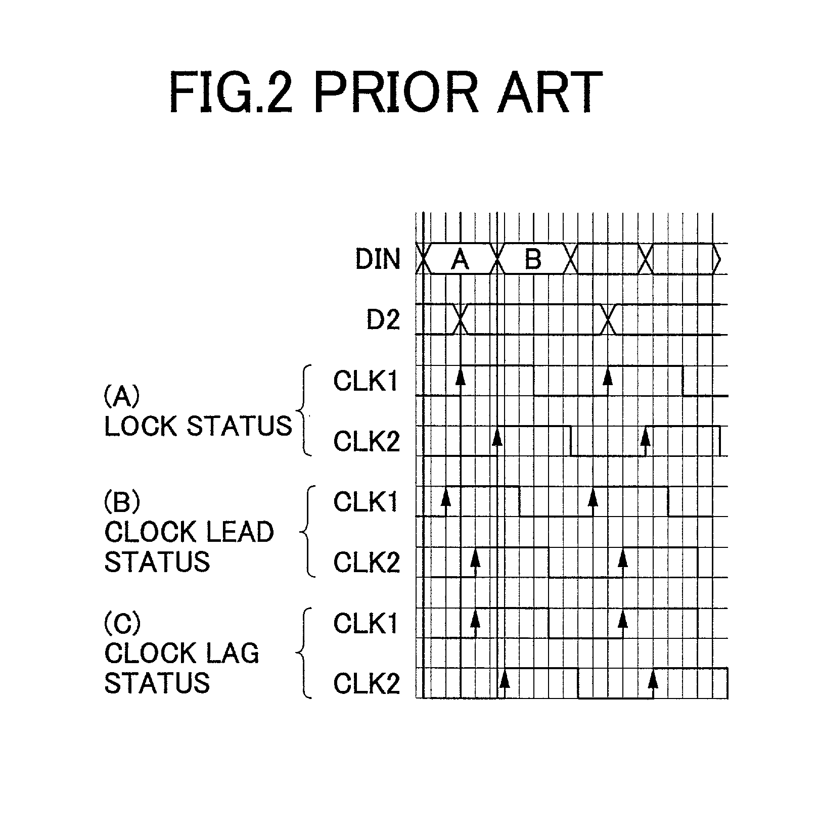
Thus, there is a large problem in that large jitter is generated.
Compared with the first conventional CDR, according to this configuration, the operation speed required for VCO becomes double and there is a problem in that speedup becomes difficult.

Method used


Image

  • Clock/data recovery circuit
  • Clock/data recovery circuit
  • Clock/data recovery circuit

Examples


first embodiment

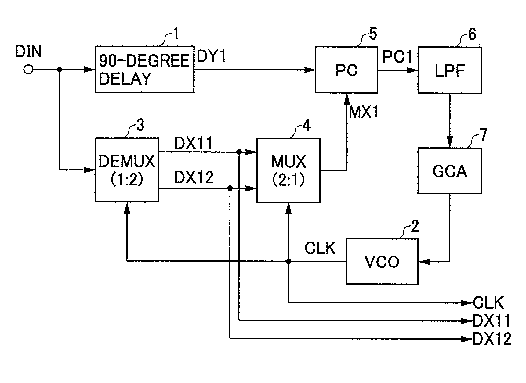
[0150]FIG. 5 shows a first embodiment of the present invention. In FIG. 5, 1 indicates a 90-degree delay circuit which delays phase of the input data signal DIN by 90-degree, 2 indicates a voltage control oscillator (VCO) which oscillates at a frequency of 1 / 2 of the bit rate of the input data signal DIN, 3 indicates a demultiplexer (DEMUX) which performs 1:2 demultiplexing operation for the input data signal DIN by using a clock signal CLK output from the voltage control oscillator 2, 4 indicates a multiplexer (MUX) which performs 2:1 multiplexing operation for the output signals DX11, DX12 from the demultiplexer 3 by using the clock signal CLK, 5 indicates an phase comparator (PC) which compares the output signal MX1 of the multiplexer 4 and the output signal DY1 of the 90-degree delay circuit 1, 6 indicates a lowpass filter (LPF) which extracts DC voltage from the output signal PC1 of the phase comparator 5, and 7 indicates a gain control amplifier (GCA) which amplifies the outpu...

second embodiment

[0155]FIG. 8 shows a second embodiment of the present invention. The same numeral is assigned for the same component as that of the first embodiment shown in FIG. 5. In this embodiment, instead of the 90-degree delay circuit 1 shown in FIG. 5, toggle-flip flop circuit (TFF) 8 is connected to input side of the phase comparator 5 as a divider which doubles the minimum pulse width of the output data signal DIN, and the circuit of this embodiment is configured such that the CLK phase timing coincides with that of the output signal FF1 of the toggle-flip flop circuit 8. In addition, a demultiplexer 9 is provided for performing 1:N demultiplexing for the input data signal DIN by using the clock signal CLK, and an m divider 10 which divides the frequency of the clock signal CLK by m (m=N / 2) and outputs the divided signal is provided. In this embodiment, the clock signal CLKm output from the m divider 10 is the recovery divided clock, and the output signals DX 21, DX 22, . . . , DX2N of the...

third embodiment

[0158]FIG. 10 shows a third embodiment of the present invention. The same numeral is assigned for the same component as that of the first embodiment shown in FIG. 5. Compared with the circuit shown in FIG. 5, a delay circuit 11 for delaying the input data signal DIN is inserted, and the output signal DY0 of the delay circuit 11 is delayed by 90-degree by using the 90-degree delay circuit 1. In addition, a phase comparator 12 which receives the output signal DY0 of the delay circuit 11, the output signal DY1 of the 90-degree delay circuit 1 and the output signal MX1 of the multiplexer 4 is used.

[0159]The phase comparator 12 compares phases of the signal DY1 and the multiplexed signal MX1, and compares the phase of a signal of the comparison result and the phase of the signal DY0 (refer to: Japanese laid-open patent application No. 6-252654 for example). According to this phase comparator 12, input-data-pattern dependence of the response can be decreased.

[0160]By this configuration, t...


PUM


Abstract

A clock / data recovery circuit used in a receiving apparatus is provided in the circuit including: a voltage control oscillator for generating a clock signal of a frequency of 1 / K of a bit rate of an input data signal; a delay circuit; a demultiplexer for demultiplexing the input data signal; a multiplexer for multiplexing the demultiplexed signals; a phase comparator for comparing phases of an output signal of the delay circuit and an output signal of the multiplexer; a lowpass filter; wherein the clock / data recovery circuit outputs the clock signal generated by the voltage control oscillator as a recovery divided clock signal, and outputs the demultiplexed signals output as recovery parallel data signals.

Description

BACKGROUND OF THE INVENTION[0001]1. Field of the Invention[0002]The present invention relates to a clock / data recovery circuit using a voltage control oscillator which generates a clock signal of a frequency corresponding to 1 / K (K=2, 3 , . . . ) of bit rate of an input data signal.[0003]2. Description of the Related Art[0004]The clock / data recovery circuit is applied to a receiver part and the like of an optical front end circuit in a router or a cross-connect switch of point to point transmission, GbE / 10GbE, Fibre Channel in an optical communication system.[0005]FIG. 1 shows a configuration of a conventional clock / data recovery circuit. This configuration is a PLL configuration using the voltage control oscillator which outputs a clock signal of a frequency of 1 / 2 of bit rate of an input data signal (refer to: M. Wurzer, et. al., “A 40-Gb / s Integrated Clock and Data Recovery Circuit in a 50-GHz Silicon Bipolar Technology,” IEEE J. Solid-State Circuits, VOL. 34, NO. 9, pp. 1320–132...

Claims


Application Information

Patent Timeline
IPC IPC(8): H04L7/00H03L7/00H04J3/07H03L7/08H04J3/04H04L7/033
CPCH03L7/08H04L7/0337H04J3/047
Inventor KISHINE, KEIJIICHINO, HARUHIKO
Owner NIPPON TELEGRAPH & TELEPHONE CORP
Learn More