Semiconductor device and method of forming the same

a memory device and semiconductor technology, applied in the direction of semiconductor devices, electrical devices, transistors, etc., to achieve the effects of improving support, reducing dielectric constant, and improving rc delay and possible collaps

Active Publication Date: 2018-07-26
UNITED MICROELECTRONICS CORP +1
View PDF4 Cites 2 Cited by
  • Summary
  • Abstract
  • Description
  • Claims
  • Application Information

AI Technical Summary

Benefits of technology

[0008]In overall speaking, the forming method of the present invention is mainly performed by forming an air-gap layer between the bit lines and the storage nodes during the forming processes of the storage nodes, with the multilayer spacer being partially etched under the coverage of the patterned metal layer formed in the previously first etching step. That is, only a part of the second layer of the multilayer spacer is removed to form the air-gap layer, and the rest part of the second layer of the multilayer spacer is remained, so as to make the air-gap layer to include plural separate fragments. The separate fragments of the air-gap layer are namely separated by the remained second layer, so that, the air-gap layer of the present invention may both achieve the lower dielectric constant and better supporting. Thus, the method of the present invention can improve the RC delay issue and the possible collapse at the same time.

Problems solved by technology

Also, the semiconductor memory device may further improve the possible collapse issues caused by the poor supporting of the air-gap layer.

Method used


Image

  • Semiconductor device and method of forming the same
  • Semiconductor device and method of forming the same
  • Semiconductor device and method of forming the same

Examples


Embodiment Construction

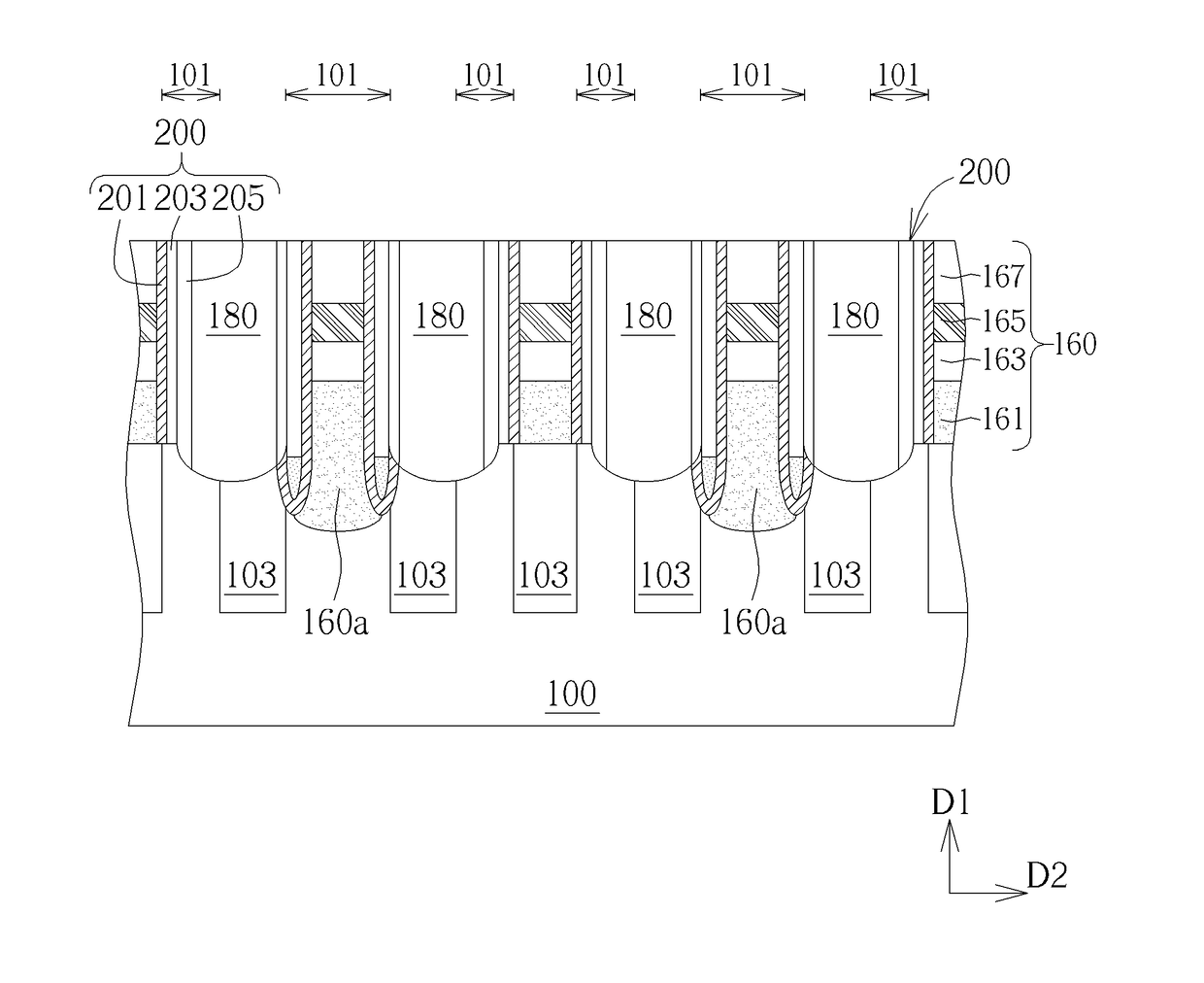
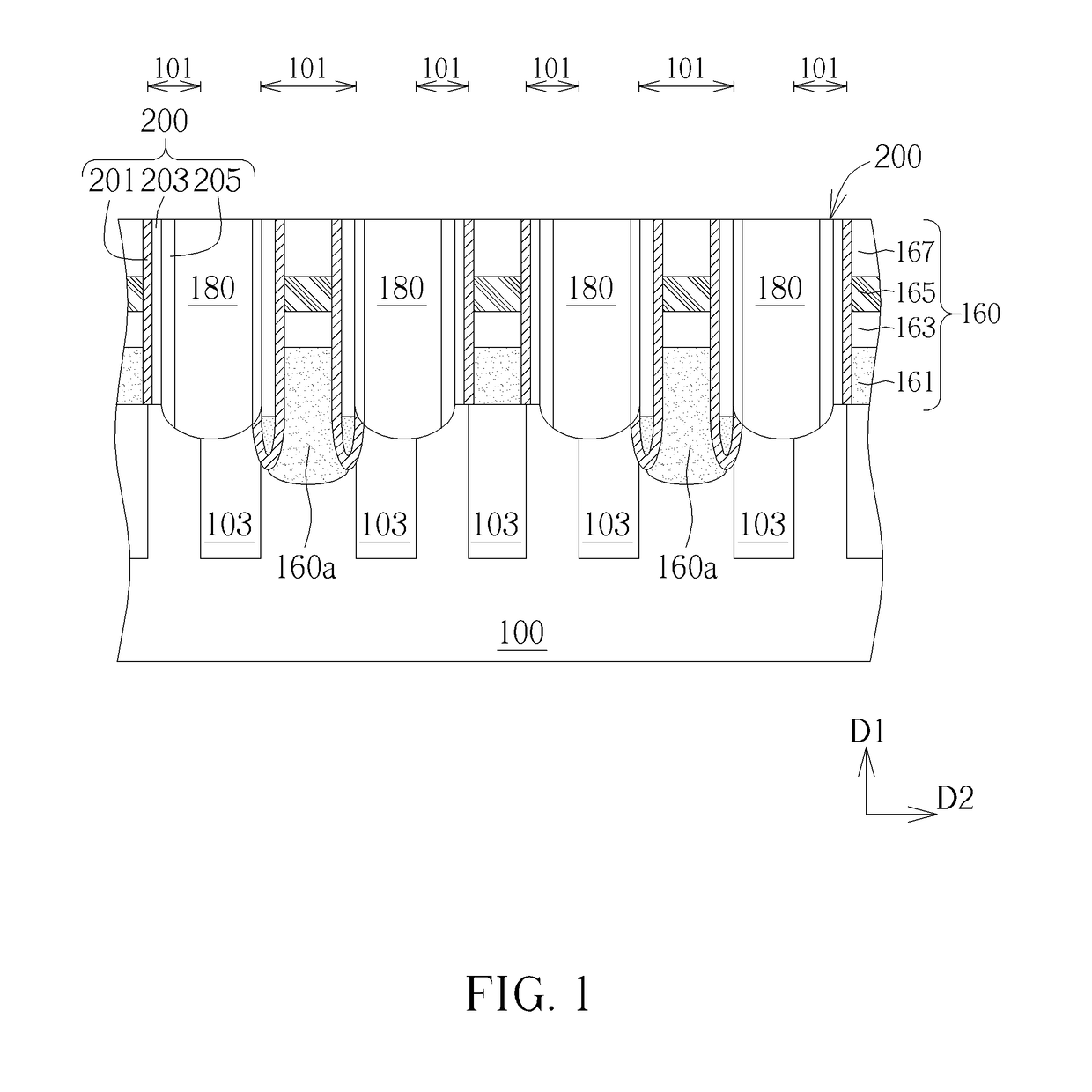
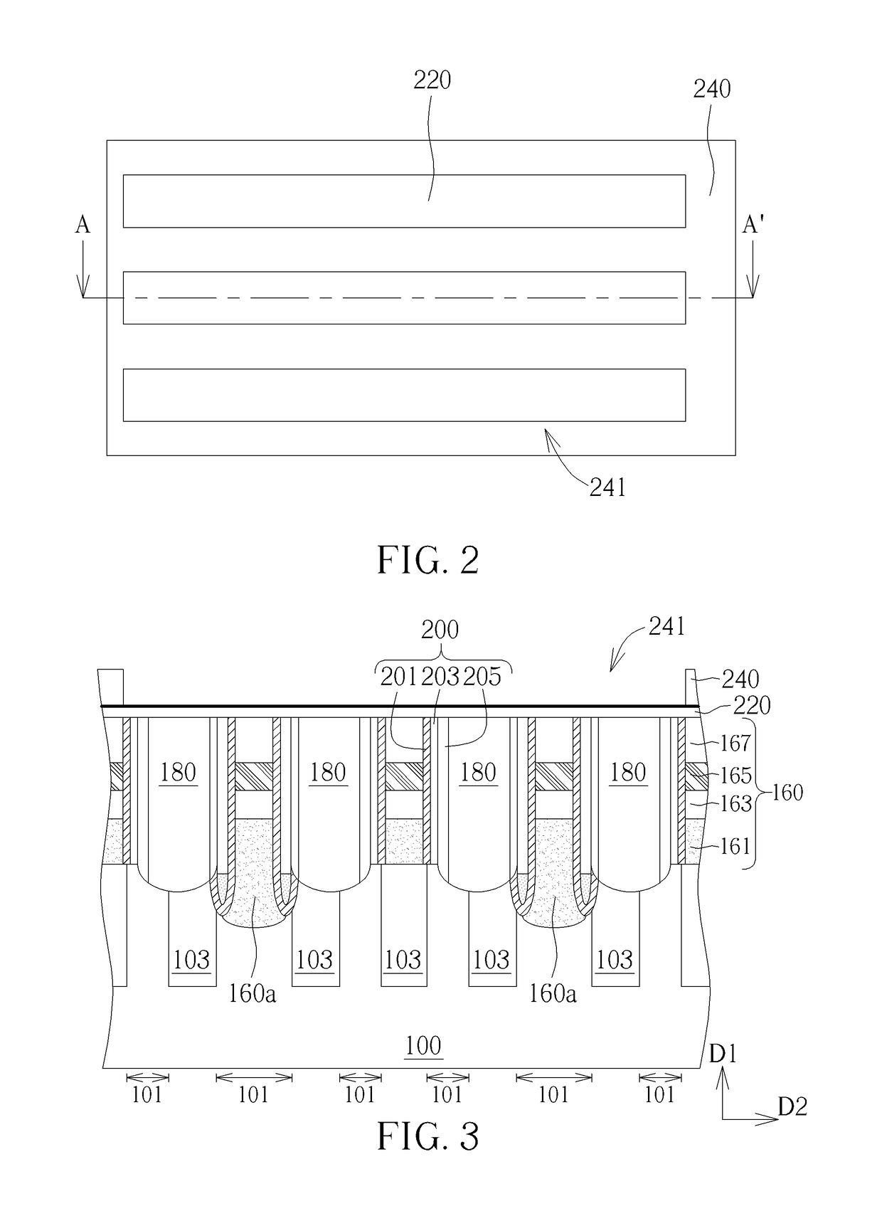
[0023]To provide a better understanding of the present invention, preferred embodiments will be described in detail. The preferred embodiments of the present invention are illustrated in the accompanying drawings with numbered elements.

[0024]Referring to FIGS. 1-11, FIGS. 1-1 illustrate a forming method of semiconductor memory device according to a first preferred embodiment of the present invention, in which FIGS. 2, 4, 7 and 9 show a top view of a semiconductor memory device during the forming process respectively, others show a cross-sectional view of a semiconductor memory device during the forming process respectively.

[0025]In the present embodiment, a method of forming a memory cell such as a dynamic random access memory (DRAM) device, is provided, and the DRAM device at least includes at least one transistor structure (not shown in the drawings) and at least one capacitor structure (not shown in the drawings), thereto serve as the smallest unit in the DRAM array for accepting...


PUM


Abstract

A semiconductor device and method of forming the same, the semiconductor device includes plural bit lines, plural conductive patterns, plural conductive pads and a spacer. The bit lines are disposed on a substrate, along a first direction. The conductive patterns are disposed on the substrate, along the first direction, wherein the conductive patterns and the bit lines are alternately arranged in a second direction perpendicular to the first direction. The conductive pads are arranged in an array and disposed over the conductive patterns and the bit lines. The spacer is disposed between the bit lines and the conductive patterns, under the conductive pads, wherein the spacers includes a tri-layered structure having a first layer, a second layer and a third layer, and the second layer includes a plurality of air gaps separated arranged along the first direction.

Description

BACKGROUND OF THE INVENTION1. Field of the Invention[0001]The present invention generally relates to the field of semiconductor memory devices and forming method thereof, and more particularly to a dynamic random access memory (DRAM) device and a forming method thereof.2. Description of the Prior Art[0002]For years the trend in the memory industry as well as the semiconductor industry has been to scale down the size of memory cells in order to increase the integration level and thus the memory capacity of DRAM chips. In a DRAM cell with a buried gate, the current leakage caused by a capacitor is often reduced or avoided thanks to a relatively long channel length beneath the buried gate. Therefore, more and more DRAM cells are equipped with buried gates rather than with a conventional planar gate structure due to their superior performances.[0003]In general, the DRAM cells with a buried gate include a transistor device and a charge storage device, which is able to accept signals from...

Claims


Application Information

Patent Timeline
Patent Type & Authority Applications(United States)
IPC IPC(8): H01L27/108H01L27/24H01L21/764H01L21/02
CPCH01L27/10885H01L27/249H01L21/764H01L21/02164H01L21/0217H10B12/30H10B12/482H10B12/485H10B12/02H10B63/845
Inventor FENG, LI-WEIWANG, YING-CHIAOLIU, TZU-TSENTSAI, TSUNG-YINGHO, CHIEN-TING
Owner UNITED MICROELECTRONICS CORP
Why Eureka
Try Eureka