Display device using semiconductor light emitting diode

a light-emitting diode and display device technology, applied in the direction of printed circuit aspects, electroluminescent light sources, electric lighting sources, etc., can solve the problems of not being able to meet the needs of customers, so as to improve the probability of correct alignment of the light-emitting device, reduce defective electrical connections, and fast response speed

Active Publication Date: 2018-08-23
LG ELECTRONICS INC
View PDF9 Cites 16 Cited by
  • Summary
  • Abstract
  • Description
  • Claims
  • Application Information

AI Technical Summary

Benefits of technology

[0008]An object of the present disclosure is to provide a structure for improving assembly reliability in the self-assembly of a semiconductor light emitting device in a display device.

Problems solved by technology

However, there exist problems such as not-so-fast response time, difficult implementation of flexibility in case of LCDs, and there exist drawbacks such as short life span, not-so-good yield as well as low flexibility in case of AMOLEDs.
However, in a large area display device using such micro LEDs, a micro LED must be arranged in a lower wiring located in each pixel region, but there exists a problem in which the arrangement is difficult due to a small size thereof.
According to the related art, self alignment using a capillary force has been used when aligning the micro LED to the lower wiring, but a probability of the self-aligned micro LED is lowered due to too weak power of the capillary force, thereby causing a problem of reducing the yield.
Furthermore, according to the related art, a single micro LED must be aligned in a single pixel region, but there is a problem that a plurality of micro LEDs are arranged in one pixel region.

Method used


Image

  • Display device using semiconductor light emitting diode
  • Display device using semiconductor light emitting diode
  • Display device using semiconductor light emitting diode

Examples


first embodiment

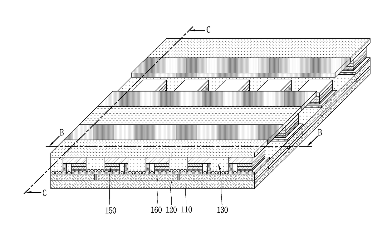
[0200]Referring to FIGS. 19 through 22, a display device includes a lower substrate 5010 at an upper portion of which a lower wiring 5011 is disposed, and at least two light emitting devices 5100 having a first electrode 5121 electrically connected to the lower wiring 5011 and a light emitting structure 5110 configured to generate light.

[0201]Furthermore, the display device according to the first embodiment further includes a second electrode 5122 located on the second conductive semiconductor layer 5113, an upper wiring 5020 electrically connected to the second electrode 5122, and a color substrate 5030 disposed on the light emitting device 5100 to convert a wavelength of light generated from the light emitting device 5100.

[0202]The lower substrate 5010 may have a film shape of an insulating material. For example, the lower substrate 5010 may be made of a transparent glass material, or may be made of a transparent plastic or a polymer film having excellent flexibility.

[0203]On the...

second embodiment

[0292]The display device 5001A of the second embodiment includes a lower substrate 5010 on which at least two lower wirings 5011 are disposed, at least two light emitting devices 5100A having a first electrode 5121 electrically connected to the lower wirings 5011 and a light emitting structure 5110 for emitting light, and a magnetic portion located at either one of the lower substrate and the light emitting device 5100A and a reaction portion located at the other one of the lower substrate and the light emitting device 5100A and a lower substrate 5010 disposed at any one of the lower substrate 5010 and the light emitting device 5100A to apply an attractive force to the magnetic portion.

[0293]In the second embodiment, the positioning partition wall 5012 of the first embodiment is omitted. In the second embodiment, one light emitting device 5100A is self-aligned in one pixel region (P) by a magnetic force acting between the magnetic portion and the reaction portion.

[0294]On the lower ...

third embodiment

[0314]FIG. 31 is a cross-sectional view of a display device according to the present disclosure.

[0315]Referring to FIG. 31, a display device 5001B according to the third embodiment further includes a second magnetic portion 5015 and a second magnetic electrode 5132 as compared with the second embodiment.

[0316]The magnetic portion may include a first magnetic portion 5014 and a second magnetic portion 5015 or include only the second magnetic portion 5015 or only the first magnetic portion 5014. FIG. 13 illustrates the magnetic portion including the first magnetic portion 5014 and the second magnetic portion 5015.

[0317]When a magnetic force of the magnetic portion is weak, a probability of correct alignment of the light emitting device 5100B may be reduced, and thus a plurality of magnetic portions may be provided. In other words, a plurality of magnetic portions are provided in one pixel region (P).

[0318]The second magnetic portion 5015 is located on a lower surface of the lower subs...


PUM

PropertyMeasurementUnit
lengthaaaaaaaaaa
sizeaaaaaaaaaa
lengthaaaaaaaaaa

Abstract

The present invention relates to a display device and, in particular, to a display device using a semiconductor light emitting diode. A display device according to the present invention comprises a substrate having a plurality of metal pads; and a plurality of semiconductor light emitting diodes electrically connected to the metal pads through self-assembly. The present invention is characterized in that: the semiconductor light emitting diodes respectively include a conductive semiconductor layer, a conductive electrode formed on one surface of the conductive semiconductor layer, and a passivation layer enclosing the semiconductor light emitting diode and provided with a through hole for exposing the conductive electrode; one end portion of the semiconductor light emitting diodes is divided into a first portion in which the conductive electrode is exposed, and a second portion in which the passivation layer is exposed; and the maximum width of the metal pad is set to a range of the width to twice the width of the second portion.

Description

BACKGROUND OF THE INVENTION1. Field of the Invention[0001]The present disclosure relates to a display device and a fabrication method thereof, and more particularly, to a flexible display device using a semiconductor light emitting device.2. Description of the Related Art[0002]In recent years, display devices having excellent characteristics such as low profile, flexibility and the like have been developed in the display technical field. On the contrary, currently commercialized main displays are represented by liquid crystal displays (LCDs) and active matrix organic light emitting diodes (AMOLEDs).[0003]However, there exist problems such as not-so-fast response time, difficult implementation of flexibility in case of LCDs, and there exist drawbacks such as short life span, not-so-good yield as well as low flexibility in case of AMOLEDs.[0004]On the other hand, light emitting diodes (LEDs) are well known light emitting devices for converting an electrical current to light, and have ...

Claims


Application Information

Patent Timeline
Patent Type & Authority Applications(United States)
IPC IPC(8): H01L33/08H01L33/38H01L33/62H05B33/10H05B33/14H05B33/22H05K1/11
CPCH01L33/08H01L33/382H01L33/62H05B33/10H05B33/14H05B33/22H05K1/111H05K2201/0145H01L25/0753H01L33/44H01L33/502Y02B20/40
Inventor PARK, CHANGSEOJEON, KISEONGPARK, JINHONGYUH, HWANKUK
Owner LG ELECTRONICS INC
Why Eureka
Try Eureka