Detection element

Active Publication Date: 2018-08-30
DAI NIPPON PRINTING CO LTD
View PDF0 Cites 2 Cited by
  • Summary
  • Abstract
  • Description
  • Claims
  • Application Information

AI Technical Summary

Benefits of technology

The patent describes a detection element that can create high-quality, high-resolution images with bright signals and strong background-to-noise ratios. It also allows for a high electric field near the pixel electrode, resulting in a high amplification ratio.

Problems solved by technology

However, in FIG. 6 of Patent Document 1, as is described above, problems such as the inability to obtain a sufficient electric field intensity or disorder of the electric field.
Due to this influence, handling in the manufacturing process becomes difficult, and the substrate warps due to internal stress of a thin film or the like formed on the substrate.
Due to this influence, the manufacturing process becomes longer and manufacturing costs also increase.
In these cases, it is not possible to obtain the effect of the detection element according to the present embodiment.

Method used


Image

  • Detection element
  • Detection element
  • Detection element

Examples


first embodiment

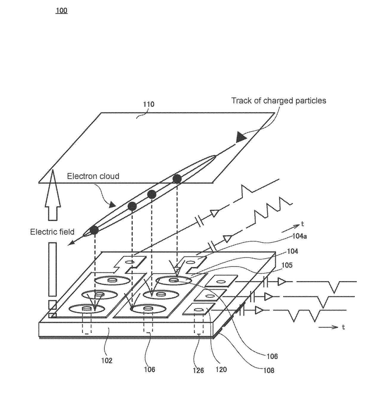
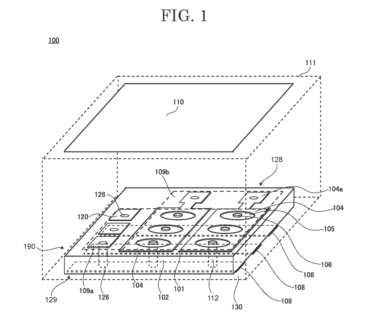
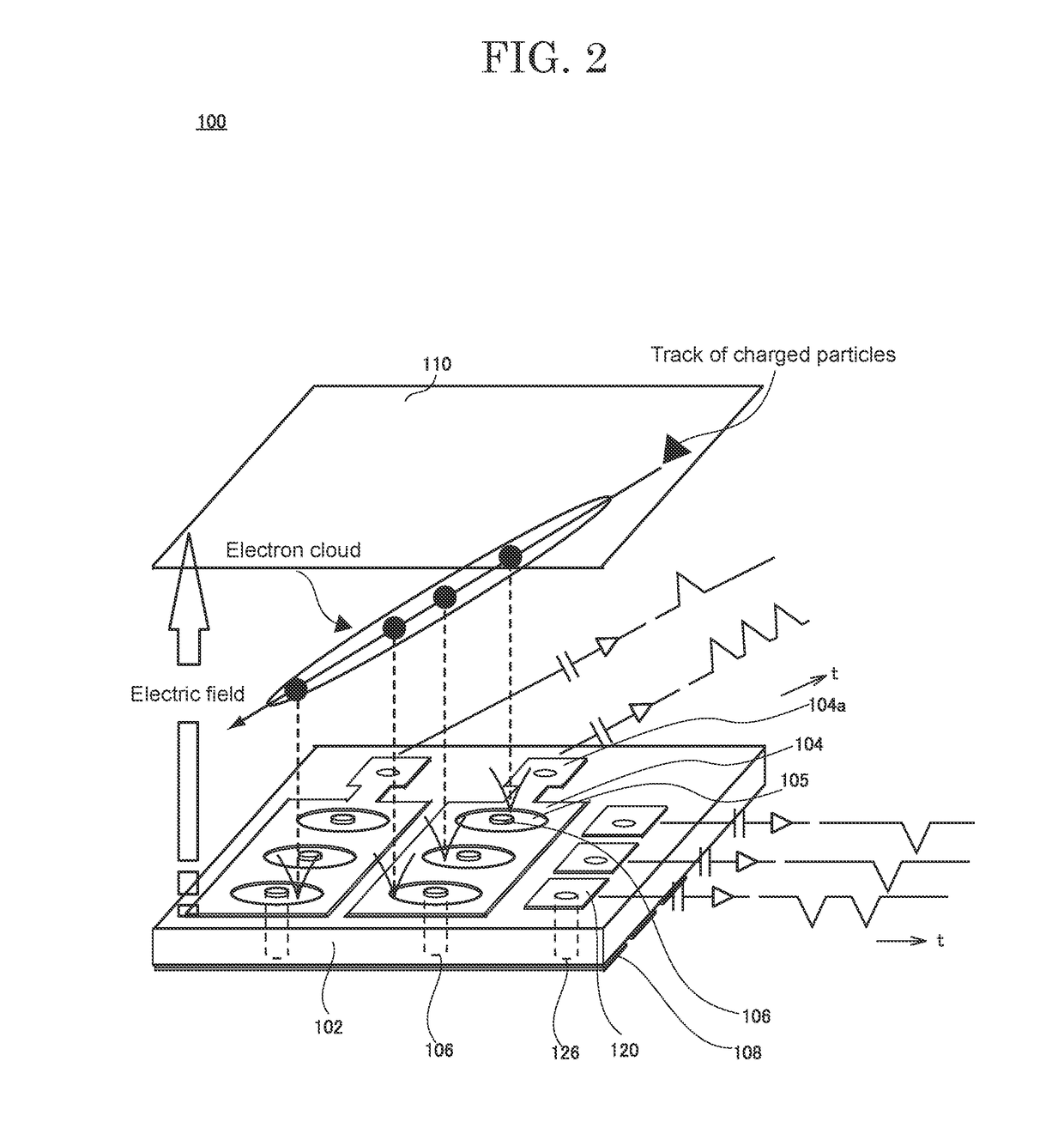
[0077]FIG. 1 shows a schematic structural diagram of a pixel electrode portion 101 of a radiation detection device 100 according to the present disclosure according to the present embodiment. The radiation detection device 100 according to the embodiment of the present disclosure includes a pixel electrode portion 101, connection terminal units 109 (109a and 109b), a drift electrode 110 and a chamber 111. The pixel electrode portion 101 and the connection terminal unit 109 (109a and 109b) are also referred to as a detection element 190.

[Structure of Radiation Detection Device 100]

[0078]The pixel electrode portion 101 of the radiation detection device 100 according to the present disclosure according to the present embodiment includes a substrate 102, a cathode electrode 104, an anode electrode 106, an anode electrode pattern 108 and a through electrode 112.

[0079]A plurality of cathode electrodes 104 are arranged on the surface (first surface 128) of the substrate 102. The cathode el...

second embodiment

[0132]The structure of the detection element according to the second embodiment of the present disclosure is explained in detail while referring to FIG. 17. In the detection element 190A used in the radiation detection device 100A according to the second embodiment, the same reference numerals are given to the same portions or portions having similar functions as those of the detection element 190 shown in FIG. 5 and an explanation thereof is omitted.

[0133]FIG. 17 is an enlarged diagram of a through electrode and an anode electrode in a cross-sectional view of a part of a detection element according to an embodiment of the present disclosure. Although the detection element 190A of the radiation detection device 100A shown in FIG. 17 is similar to the detection element 190 of the radiation detection device 100 shown in FIG. 5, the detection element 190A of the radiation detection device 100A is different in that a first insulating layer 134A and a second insulating layer 136A are arr...

third embodiment

[0136]The structure of the detection element according to the third embodiment of the present disclosure is explained in detail while referring to FIG. 18. In the detection element 190B used in the radiation detection device 100 B according to the third embodiment, the same reference numerals are given to the same portions or portions having similar functions as those of the detection element 190 shown in FIG. 5 and an explanation thereof is omitted.

[0137]FIG. 18 is an enlarged diagram of a through electrode and an anode electrode in a cross-sectional view of a part of a detection element according to one embodiment of the present disclosure. Although the detection element 190B of the radiation detection device 100B shown in FIG. 18 is similar to the detection element 190 of the radiation detection device 100 shown in FIG. 5, it is different in that the detection element 190B of the radiation detection device 100B is arranged with a first insulating layer 134B, second insulating lay...


PUM


Abstract

A detection element can obtain a high-resolution radiation image having a high signal intensity and a high S / N ratio. A detection element including a substrate having a through hole, an insulating layer arranged inside of the through hole, a through electrode arranged further to the inner side of the through hole than the insulating layer, a resin layer having insulating properties and having an opening portion exposing the through electrode, a first electrode arranged above the through electrode and the resin layer, the first electrode being connected to the through electrode through the opening portion, and a second electrode arranged above the resin layer, the second electrode being separated from the first electrode.

Description

CROSS REFERENCE TO RELATED APPLICATIONS[0001]This application is a U.S. continuation application filed under 35 U.S.C. § 111(a), of International Application No. PCT / JP2016 / 079110, filed on Sep. 30, 2016, which claims priority to Japanese Patent Application No. 2015-200561 filed on Oct. 8, 2015 and Japanese Patent Application No. 2015-201243, filed on Oct. 9, 2015, the disclosures of which are incorporated by reference.FIELD[0002]The present invention relates to a detection element.BACKGROUND[0003]Research into gas electron amplification type radiation detectors using pixel type electrodes is proceeding. In radiation detection by a conventional detector, large area and real-time imaging can not be sufficiently realized in image imaging of the detection region. On the other hand, the gas electron amplification type radiation detector is characterized by being capable of real-time image imaging with a large area.[0004]Regarding the structure of the gas electron amplification type radi...

Claims


Application Information

Patent Timeline
IPC IPC(8): G01T1/185
CPCG01T1/185H01J47/06
Inventor OTA, KOHEIMOTOMURA, TOMOHISATAKANO, TAKAMASANAKAYAMA, KOICHI
Owner DAI NIPPON PRINTING CO LTD
Why Eureka
Try Eureka