Semiconductor substrate and semiconductor device

a semiconductor and substrate technology, applied in the direction of semiconductor devices, basic electric elements, electrical appliances, etc., can solve the problems of channel depletion, significant decrease of current in saturation region, and large increase in turn on delay, so as to prevent an increase in parasitic capacitance and effectively disperse high electric field

Active Publication Date: 2019-02-26
NUVOTON
View PDF10 Cites 0 Cited by
  • Summary
  • Abstract
  • Description
  • Claims
  • Application Information

AI Technical Summary

Benefits of technology

[0005]Accordingly, the present invention provides a semiconductor substrate and a semiconductor device, so as to effectively disperse the high electric field and prevent an increase in parasitic capacitance caused by the conventional metal field plate.
[0025]Based on the above, the aggregation effect of high electric field between electrodes can be effectively dispersed by the disposition of the buried field plate region of the present invention. Moreover, the buried field plate region of the present invention is buried in the channel layer, so an additional field plate above the electrodes is not required, and the complexity of the manufacturing process is accordingly reduced. Besides, the semiconductor device of the present invention does not require a metal field plate, and therefore, the effect of parasitic capacitance on the device can be significantly reduced.

Problems solved by technology

A field effect transistor is easy to suffer current collapse during a high frequency or high power operation, and thus, current in a saturation region is significantly decreased and turn on delay is greatly increased.
Therefore, when the device is operated at a high frequency, the trapped electrons may be unable to escape from where they are trapped, and thus, the channel may be depleted and the current collapse may occur.
However, the parasitic capacitance of the device is greatly increased accordingly.

Method used


Image

  • Semiconductor substrate and semiconductor device
  • Semiconductor substrate and semiconductor device
  • Semiconductor substrate and semiconductor device

Examples


Embodiment Construction

[0048]Reference will now be made in detail to the present preferred embodiments of the invention, examples of which are illustrated in the accompanying drawings. Wherever possible, the same reference numbers are used in the drawings and the description to refer to the same or like elements.

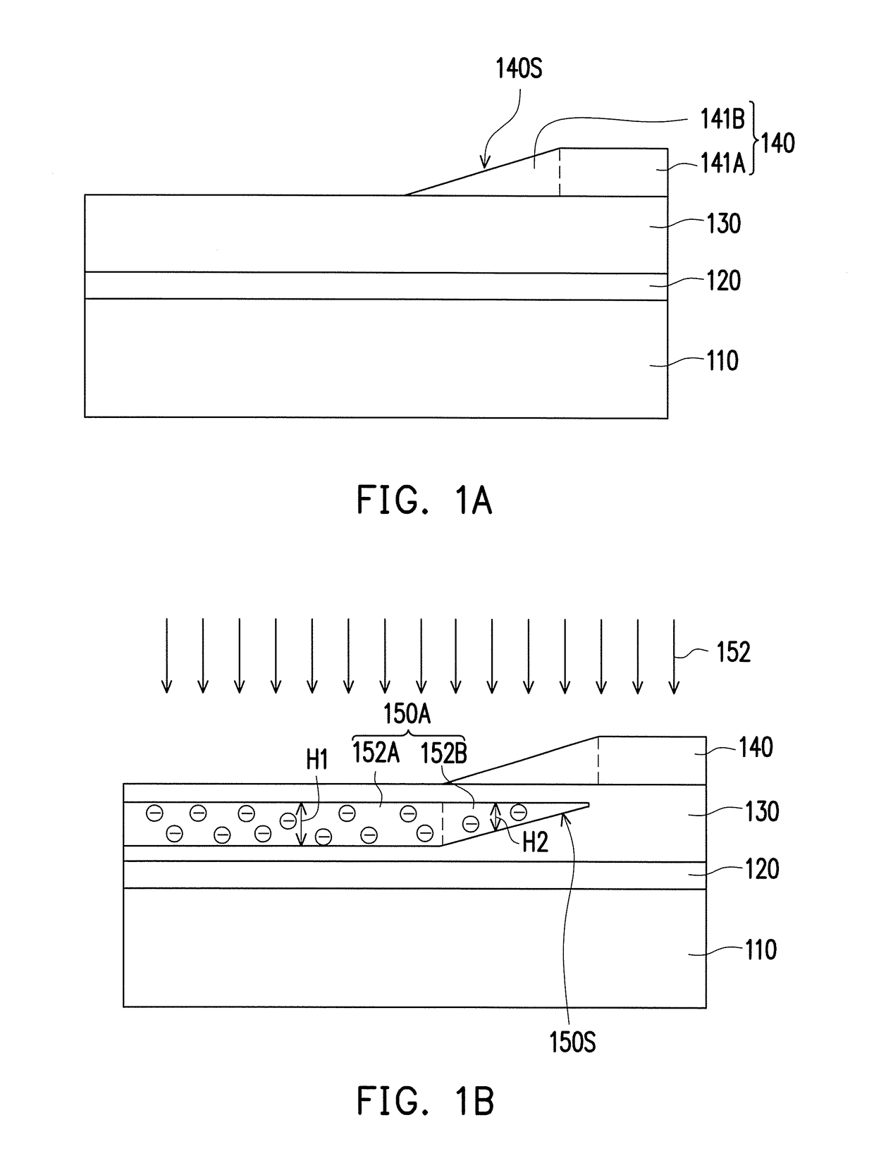
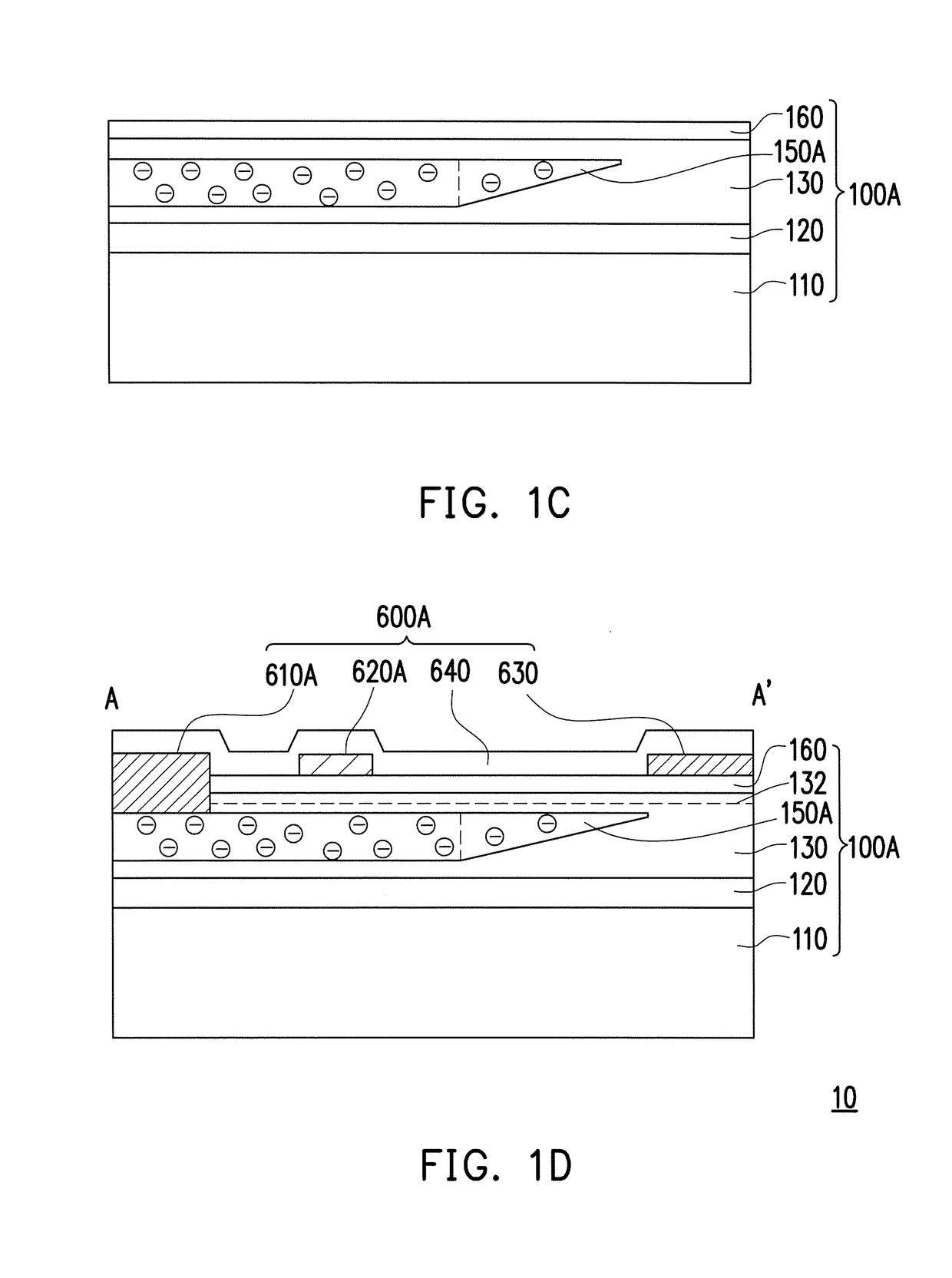
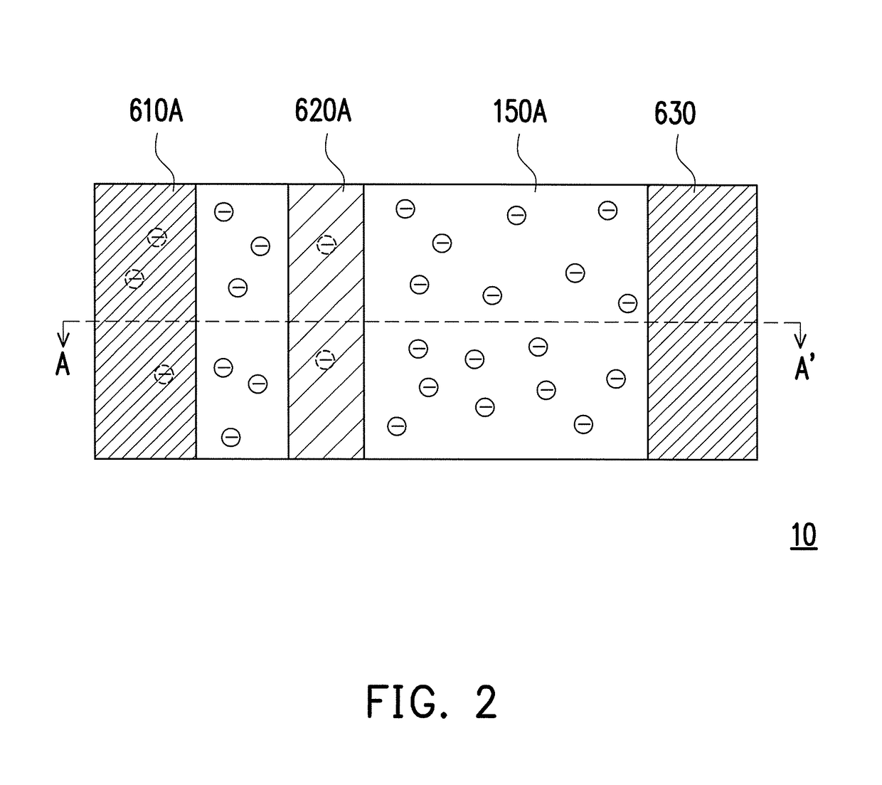
[0049]FIG. 1A to FIG. 1D are schematic cross-sectional views of a method of forming a semiconductor device in accordance with an embodiment of the present invention. FIG. 2 is a simplified top view of FIG. 1D. For clarity of illustration, only the relative position of the electrodes and the buried field plate region are shown in FIG. 2, and other components are omitted.

[0050]Referring to FIG. 1A, a base layer 110 is provided. In an embodiment, the base layer 110 includes silicon. Thereafter, a buffer layer 120 and a channel layer 130 are sequentially formed on the base layer 110. In an embodiment, the buffer layer 120 includes aluminum nitride (AlN), and the channel layer 130 includes gallium nitr...


PUM


Abstract

A semiconductor substrate and a semiconductor device are disclosed. The semiconductor substrate includes a base layer, a buffer layer disposed on the base layer, a channel layer disposed on the buffer layer, a barrier layer disposed on the channel layer, and a buried field plate region embedded in the channel layer. In an embodiment, the channel layer includes a two-dimensional electron gas (2DEG), and the buried field plate region is located below the two-dimensional electron gas.

Description

CROSS-REFERENCE TO RELATED APPLICATION[0001]This application claims the priority benefit of Taiwan application serial no. 105142128, filed on Dec. 20, 2016. The entirety of the above-mentioned patent application is hereby incorporated by reference herein and made a part of this specification.BACKGROUND OF THE INVENTIONField of Invention[0002]The present invention relates to a semiconductor substrate and a semiconductor device.Description of Related Art[0003]A field effect transistor is easy to suffer current collapse during a high frequency or high power operation, and thus, current in a saturation region is significantly decreased and turn on delay is greatly increased. This phenomenon occurs because a large number of electrons are captured in trap states of the semiconductor surface when the device is operated in a high electric field. It takes time for the captured electrons to escape from the trap states. Therefore, when the device is operated at a high frequency, the trapped el...

Claims


Application Information

Patent Timeline
Patent Type & Authority Patents(United States)
IPC IPC(8): H01L29/06H01L29/778H01L29/66H01L21/266H01L29/40H01L29/20H01L21/265H01L29/417H01L29/423
CPCH01L29/7787H01L21/266H01L29/0623H01L29/0688H01L29/407H01L29/7786H01L29/66462H01L29/42316H01L21/26553H01L29/2003H01L29/404H01L29/41766H01L29/7781
Inventor CHEN, CHIH-WEILIN, HENG-KUANG
Owner NUVOTON
Why Eureka
Try Eureka