Display device, and driving method of display device

a display device and active matrix technology, applied in the direction of instruments, computing, electric digital data processing, etc., can solve the problem of easy deformation of the transistor, and achieve the effect of improving the reliability of the display device, preventing the degaradation of the transistor due to the hot carrier effect, and improving the reliability of the switching elemen

Inactive Publication Date: 2012-06-12
SEMICON ENERGY LAB CO LTD
View PDF13 Cites 0 Cited by
  • Summary
  • Abstract
  • Description
  • Claims
  • Application Information

AI Technical Summary

Benefits of technology

[0014]Note that providing LDD (lightly doped drain) region in the transistor is effective method in suppressing hot carrier effect. However, improvement of the structure of the transistor like providing LDD region causes complication of the manufacturing steps and further variations of transistor characteristics. Therefore, there is a limitation to suppress change of the threshold voltage due to hot carrier effect by improving the structure of the transistor.
[0015]In the view of the above mentioned problem, it is an object of the present invention to provide a highly reliable display device and a driving method of the display device which can suppress to generate high electric field near the drain of the transistor used as a switching element.
[0019]In the present invention, absolute value of the voltage between the source and the drain of the transistor used as a switching element in the writing period can be suppressed than that of a conventional display device which is driven as shown FIG. 21 and a display device which is driven as shown in reference 1. Therefore, degaradation of the transistor due to the hot carrier effect can be prevented by suppressing the generation of high electric field near the drain of the transistor. Further, by the structure of the present invention, reliability of the switching element and furthermore reliability of the display device can be improved.

Problems solved by technology

However, in the case of a display device using a transistor as a switching element, there is a problem that the transistor is easy to degrade by performing AC drive.

Method used


Image

  • Display device, and driving method of display device
  • Display device, and driving method of display device
  • Display device, and driving method of display device

Examples


embodiment mode 2

[Embodiment Mode 2]

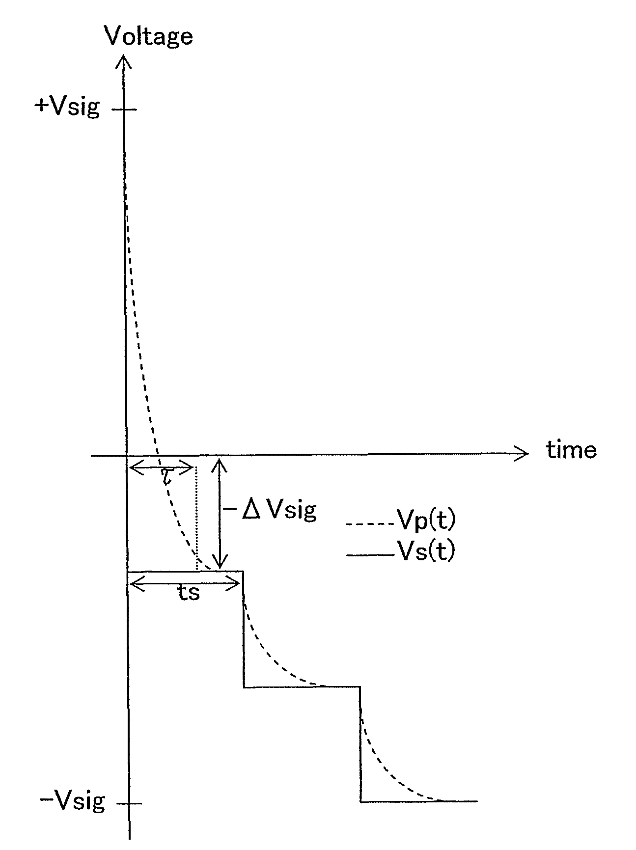
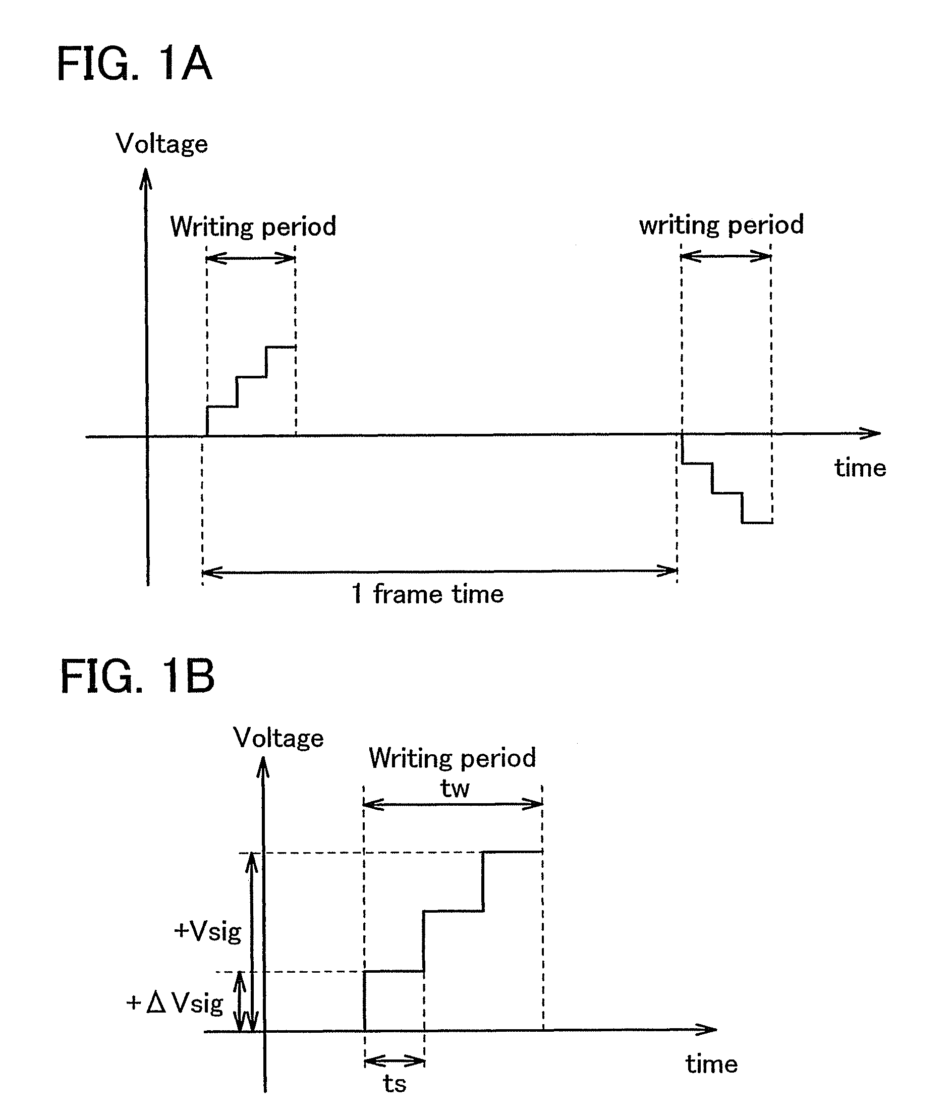
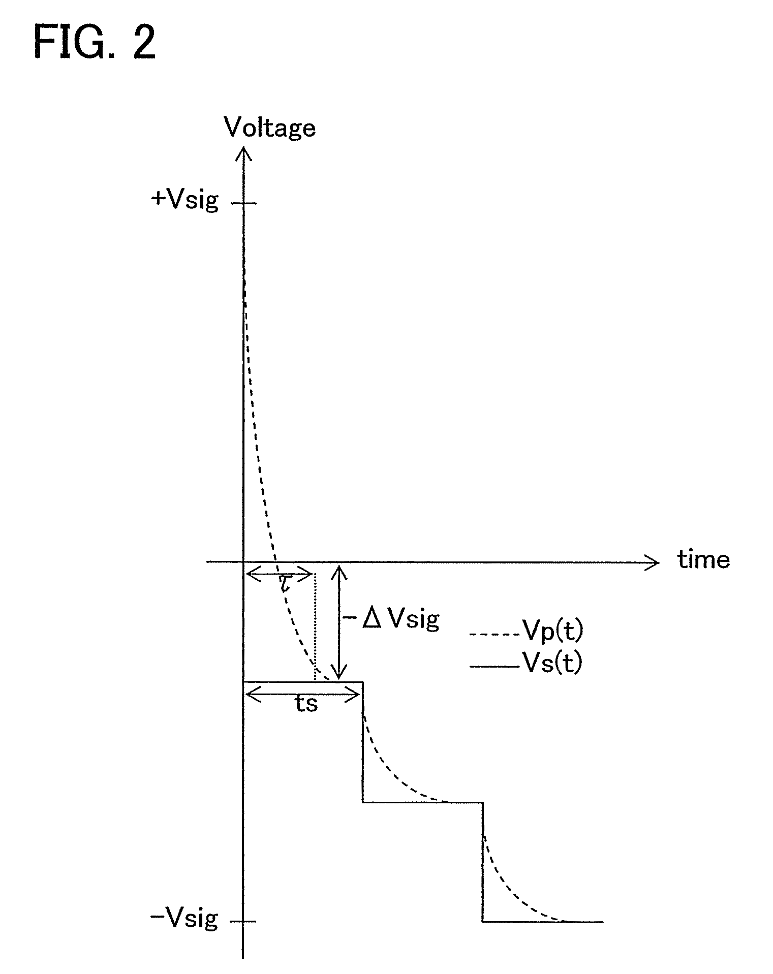
[0092]A driving method different from embodiment mode 1 is described with reference to FIGS. 4A and 4B. FIG. 4A is a timing chart of the voltage applied to the signal line of the present invention. In FIG. 4A, the video signal +Vsig is applied to the signal line Si step by step in the writing period appeared first similar to Embodiment Mode 1. FIG. 4B is an enlarged view of the timing chart of the writing period appeared first in FIG. 4A.

[0093]As shown in FIG. 4B, once the writing period is begun, the voltage of the signal line is changed by +ΔVsig first. Note that, |ΔVsig|sig| is satisfied. Then, in this embodiment mode, the voltage of the signal line is changed so that the change of charge stored in the above capacitance Cs and Cl is easy to follow the change of the voltage of the signal line. Specifically, although the voltage is risen by +ΔVsig so that the waveform of the voltage is rectangle in Embodiment 1, rise of the voltage in this Embodiment is delayed b...

embodiment mode 3

[Embodiment Mode 3]

[0119]This embodiment mode will describe a specific calculation of relaxation time of charge accumulation.

[0120]The relaxation time τ is calculated when it is assumed that the wiring resistance is negligible small in a pixel, and the resistance R in the pixel is caused by a transistor used as a switching element. Since the transistor for switching is operated in the linear region mode, the resistance in the channel formation region of the transistor can be represented by the following equation 44. Note that in the equation 44, Vgs and Vth represent the voltage (gate voltage) between the gate and source which is applied to the transistor and the threshold voltage, respectively. In addition, L and W represent the length of the channel and the width of the channel, respectively, μ represents the mobility, and Cox represents gate capacitance per unit area of the transistor.

R=1 / β(Vgs−Vth) Note that β=(L / W)×μ×Cox   (Equation 44)

[0121]Next, when it is assumed that the ca...

embodiment mode 4

[Embodiment Mode 4]

[0124]In this embodiment mode, a structure of a display device of the invention is described. FIG. 7A is a block diagram of a display device in this embodiment mode. The display device shown in FIG. 7A includes a pixel portion 100 which includes a plurality of pixels each provided with a display element, a scanning line driver circuit 110 which selects the pixels per line, and a signal line driver circuit 120 which controls input of video signals to the pixels in a selected line.

[0125]In FIG. 7A, the signal line driver circuit 120 includes a shift register 121, a first latch 122, a second latch 123, and a level shifter 124. The clock signal S-CLK, the start pulse signal S-SP, and the scanning direction switching signal L / R are inputted to the shift register 121. The shift register 121 generates a timing signal, pulses of which are sequentially shifted, in accordance with the clock signal S-CLK and the start pulse signal S-SP and outputs the timing signal to the fi...


PUM


Abstract

It is an object to provide a high reliable display device which can suppress the generation of high electric field near the drain of the transistor used as a switching element and a driving method thereof. A relaxation time when charge is stored in the display element of the pixel and other capacitors connected to the display element in parallel is focused on, and the voltage applied between the source and the drain of the transistor in the writing period is suppressed by changing the video signal applied to the signal line step by step and finally setting it at the desired level.

Description

BACKGROUND OF THE INVENTION[0001]1. Field of the Invention[0002]The present invention relates to an active matrix display device and driving method thereof.[0003]2. Description of the Related Art[0004]In an active matrix display device, switching elements and display elements are provided in hundreds of thousands to several millions of pixels arranged in matrix. Since application of voltage or supply of current is kept for a while by the switching elements after a video signal is inputted to a pixel, active matrix display device can respond flexibly to enlargement of display panels and high definition of display image; thus, active matrix display device is becoming mainstream.[0005]A typical driver circuit of the above display device includes a scan line driver circuit and a signal line driver circuit. By the scan line driver circuit, a plurality of pixels are selected per one line or per a plurality of lines in some cases. Then, by the signal line driver circuit, input of a video s...

Claims


Application Information

Patent Timeline
Patent Type & Authority Patents(United States)
IPC IPC(8): G06F3/038G09G5/00
CPCG09G3/3648G09G3/2022G09G3/3614G09G2320/043G09G2310/06G09G2310/08G09G3/3696G02F1/133G09G3/20G09G3/36
Inventor HONDA, TATSUYA
Owner SEMICON ENERGY LAB CO LTD
Why Eureka
Try Eureka