Drive device for semiconductor element

Active Publication Date: 2018-09-20
FUJI ELECTRIC CO LTD
View PDF2 Cites 6 Cited by
  • Summary
  • Abstract
  • Description
  • Claims
  • Application Information

AI Technical Summary

Benefits of technology

[0014]The modification of drive capability of the IGBT 3 based on the chip temperature as described above is a protective operation performed internally in the IPM 2. In other words, the modification control of the drive capability of the IGBT 3 is performed independently of the ON/OFF driving of the IGBT 3 with the duty determin

Problems solved by technology

However, the aforementioned abnormality detection information is merely output from the IPM 2, and thus it is impossible to ascertain the reason fo

Method used


Image

  • Drive device for semiconductor element
  • Drive device for semiconductor element
  • Drive device for semiconductor element

Examples


Embodiment Construction

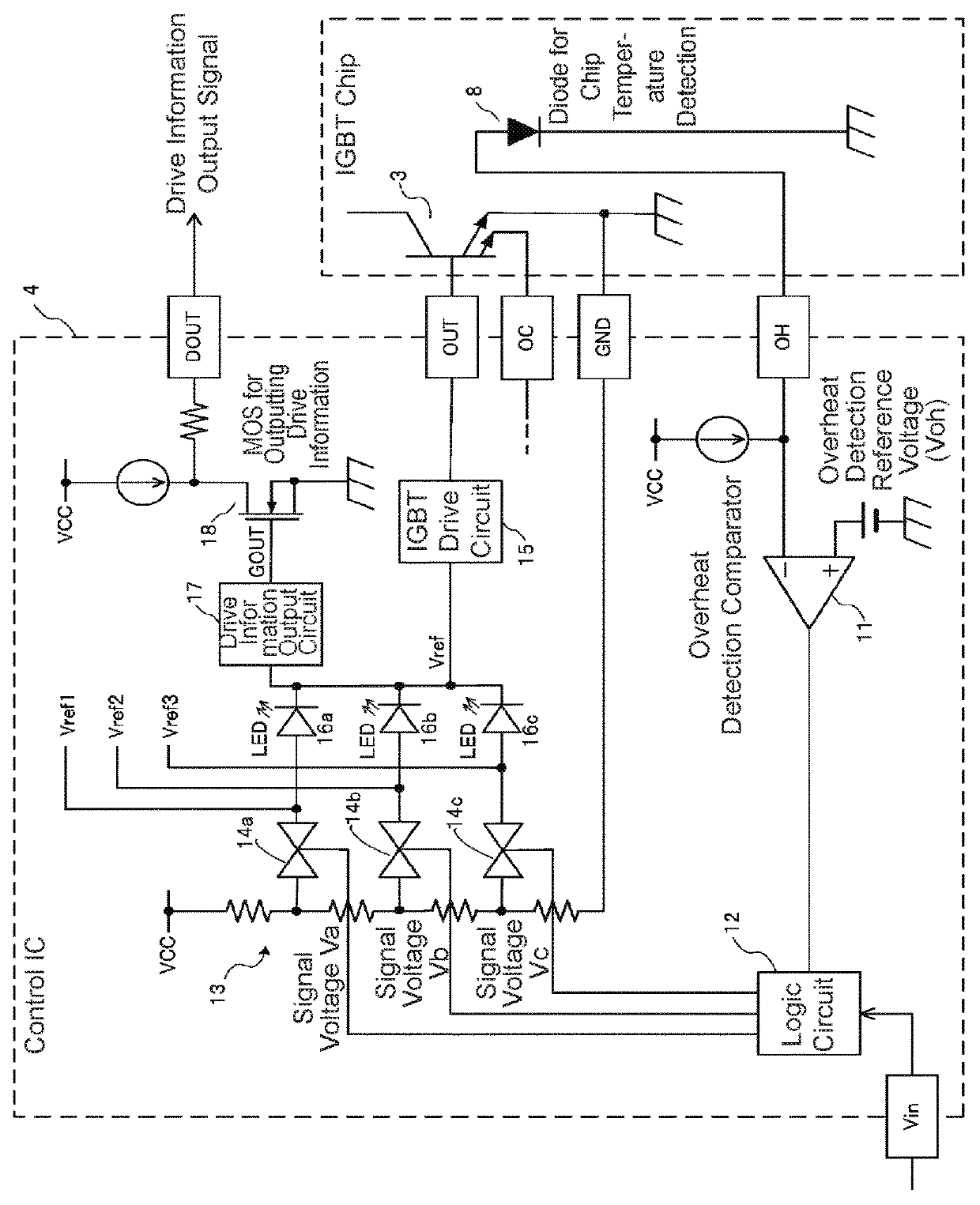
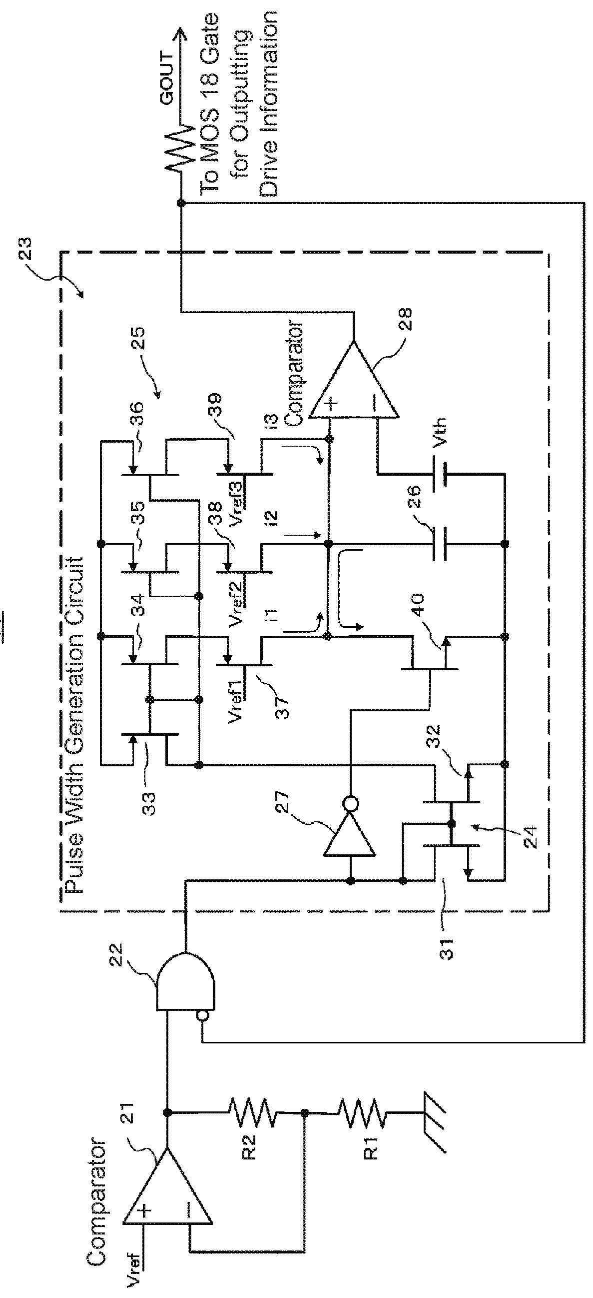
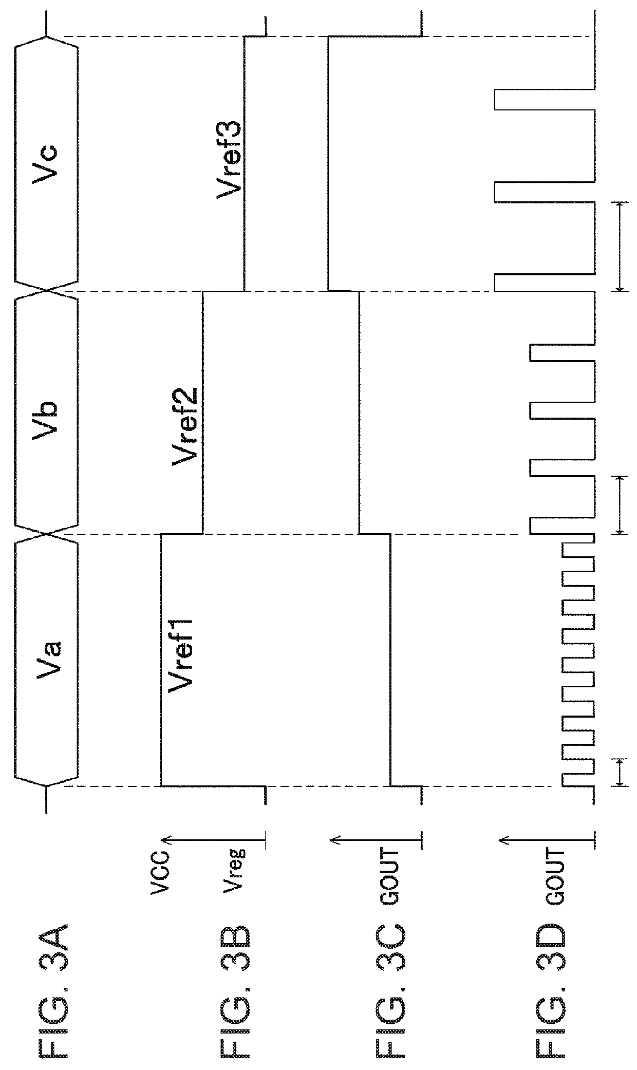
[0032]A drive device for a semiconductor element according to one embodiment of the present disclosure will be described below with reference to the drawings.

[0033]FIG. 1 is a view of a schematic configuration of the main part of an IPM 2, which is the drive device for the semiconductor element in one embodiment of the present invention. Similar to the IPM 2 shown in FIG. 5, the IPM (drive device) 2 is mainly constituted by an IGBT 3, which is a semiconductor element for power conversion, and a control IC 4, which is a drive circuit for the semiconductor element. The same reference characters will be given to the parts that are the same as the configuration of the IPM 2 shown in FIG. 5, and redundant explanations of such parts will be omitted. The IGBT 3 is provided with a diode 8 for chip temperature detection to form a chip, and the drive circuit of the IGBT 3, the overheat detection comparator 11 and logic circuit 12 described above, the IGBT drive circuit 15, and the like are fo...


PUM


Abstract

A drive device for a semiconductor element includes a drive circuit receiving from outside a pulsed drive signal for driving ON/OFF of the semiconductor element; and a protection circuit receiving a signal representing a chip temperature of the semiconductor element and, when the detected chip temperature exceeds an overheating threshold temperature, controlling operation of the drive circuit so as to adjust a drive control voltage that is provided to the semiconductor element; and a drive information output circuit externally outputting drive information corresponding to the adjusted drive control voltage that is provided to the semiconductor element by the drive circuit.

Description

BACKGROUND OF THE INVENTIONTechnical Field[0001]The present invention relates to a drive device for a semiconductor element capable of accurately externally outputting information that indicates a drive state corresponding to a chip temperature of the semiconductor element.Background Art[0002]A drive device for a semiconductor element, which forms a power conversion device such as an inverter, functions to drive ON / OFF of a semiconductor element such as an insulated gate bipolar transistor (IGBT) to perform power conversion. There has been particular interest lately in so-called intelligent power modules (IPMs) as drive devices for semiconductor elements. An IPM includes, for example, an IGBT and a drive circuit therefor, and in addition, a protection circuit to prevent destruction of the IGBT etc. due to overcurrent, overvoltage, overheating, or the like, all of which are modularized as a single electronic component in the IPM.[0003]FIG. 4 is a view of a schematic configuration sho...

Claims


Application Information

Patent Timeline
IPC IPC(8): H03K17/14
CPCH03K17/14H02M1/08H03K17/0828H03K17/567H03K2217/0036H03K2017/0806H03K17/78
Inventor TERASHIMA, KENSHI
Owner FUJI ELECTRIC CO LTD
Why Eureka
Try Eureka