Exposure apparatus and exposure method, and flat panel display manufacturing method

a technology of exposure apparatus and manufacturing method, which is applied in the direction of microlithography exposure apparatus, photomechanical treatment, instruments, etc., can solve the problem of becoming difficult to prepare a scale that can cover the entire moving range of the substra

Active Publication Date: 2018-10-04
NIKON CORP
View PDF4 Cites 9 Cited by
  • Summary
  • Abstract
  • Description
  • Claims
  • Application Information

AI Technical Summary

Benefits of technology

[0007]According to a first aspect of the present invention, there is provided an exposure apparatus that exposes a substrate with an illumination light via a projection optical system, comprising: a movable body arranged below the projection optical system that holds the substrate; a drive system that can move the movable body in a first direction and a second direction orthogonal to each other within a predetermined plane orthogonal to an optical axis of the projection optical system; a measurement system in which one of a grating member with a plurality of grating areas arranged mutually apart in the first direction and a plurality of first heads each irradiating the grating member with a measurement beam that can move in the second direction is provided at the movable body, and the other of the grating member and the plurality of first heads is provided facing the movable body, the measurement system having a measurement device that measures position information of the plurality of first heads in the second direction, the measurement system measuring position information of the movable body in at least directions of three degrees of freedom within the predetermined plane, based on measurement information of at least three first heads irradiating at least one of the plurality of grating areas with the measurement beam of the plurality of first heads and measurement information of the measurement device; and a control system, controlling the drive system based on correction information to compensate for measurement error of the measurement system occurring due to at least one of the grating member, the plurality of first heads, and movement of the movable body, and position information measured with the measurement system, wherein with each of the plurality of first heads, the measurement beam moves off of one of the plurality of grating areas, and moves to irradiate another grating area adjacent to the one of the plurality of grating areas, while the movable body is moving in the first direction.

Problems solved by technology

While the influence of air fluctuation mentioned above can be reduced using an encoder system, due to the increasing size of substrates in recent years, it is becoming difficult to prepare a scale that can cover the entire moving range of the substrate.

Method used


Image

  • Exposure apparatus and exposure method, and flat panel display manufacturing method
  • Exposure apparatus and exposure method, and flat panel display manufacturing method
  • Exposure apparatus and exposure method, and flat panel display manufacturing method

Examples


first embodiment

[0037]Hereinafter, a first embodiment will be described, using FIGS. 1 to 16B.

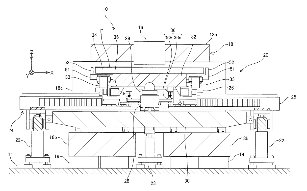
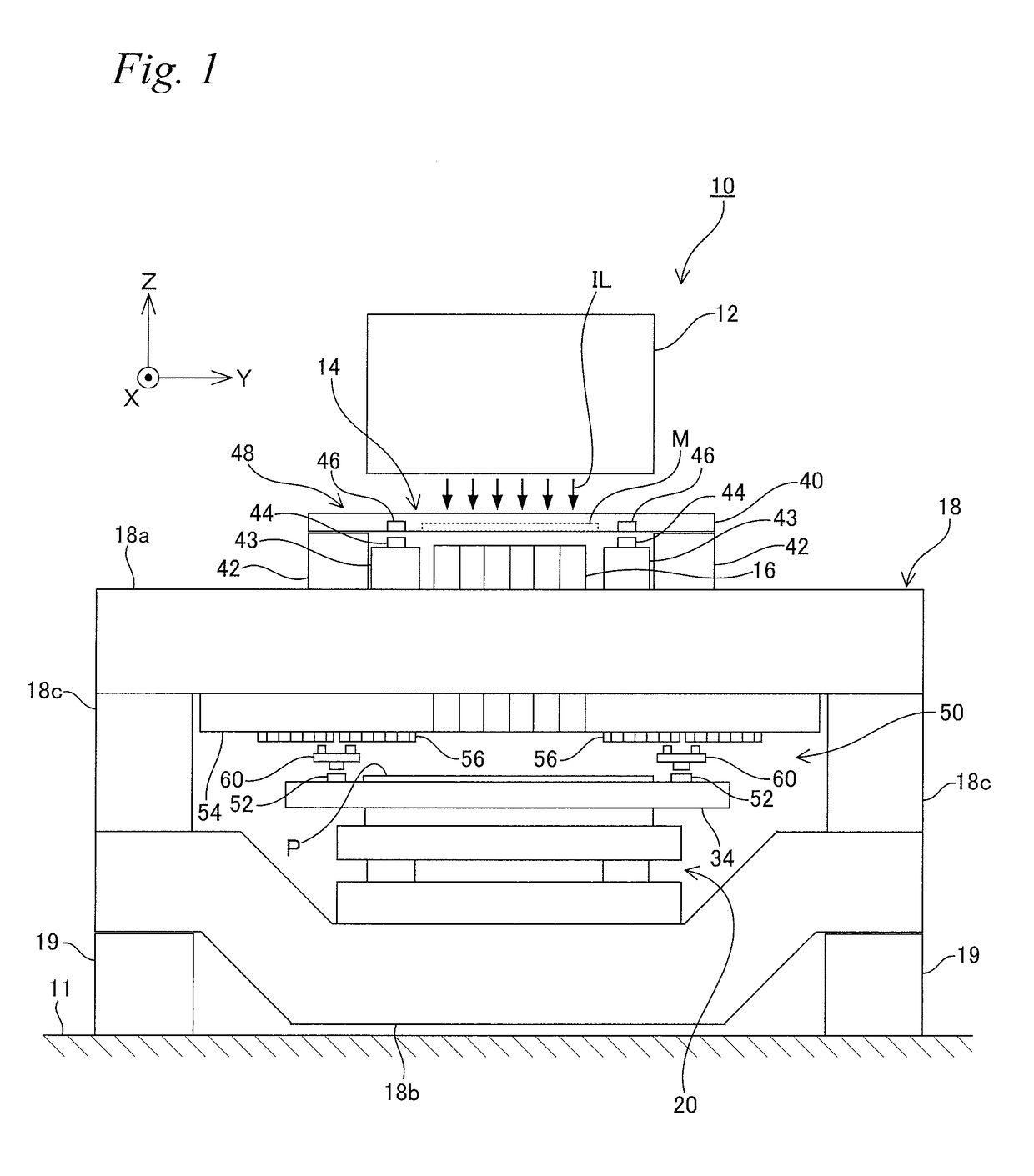
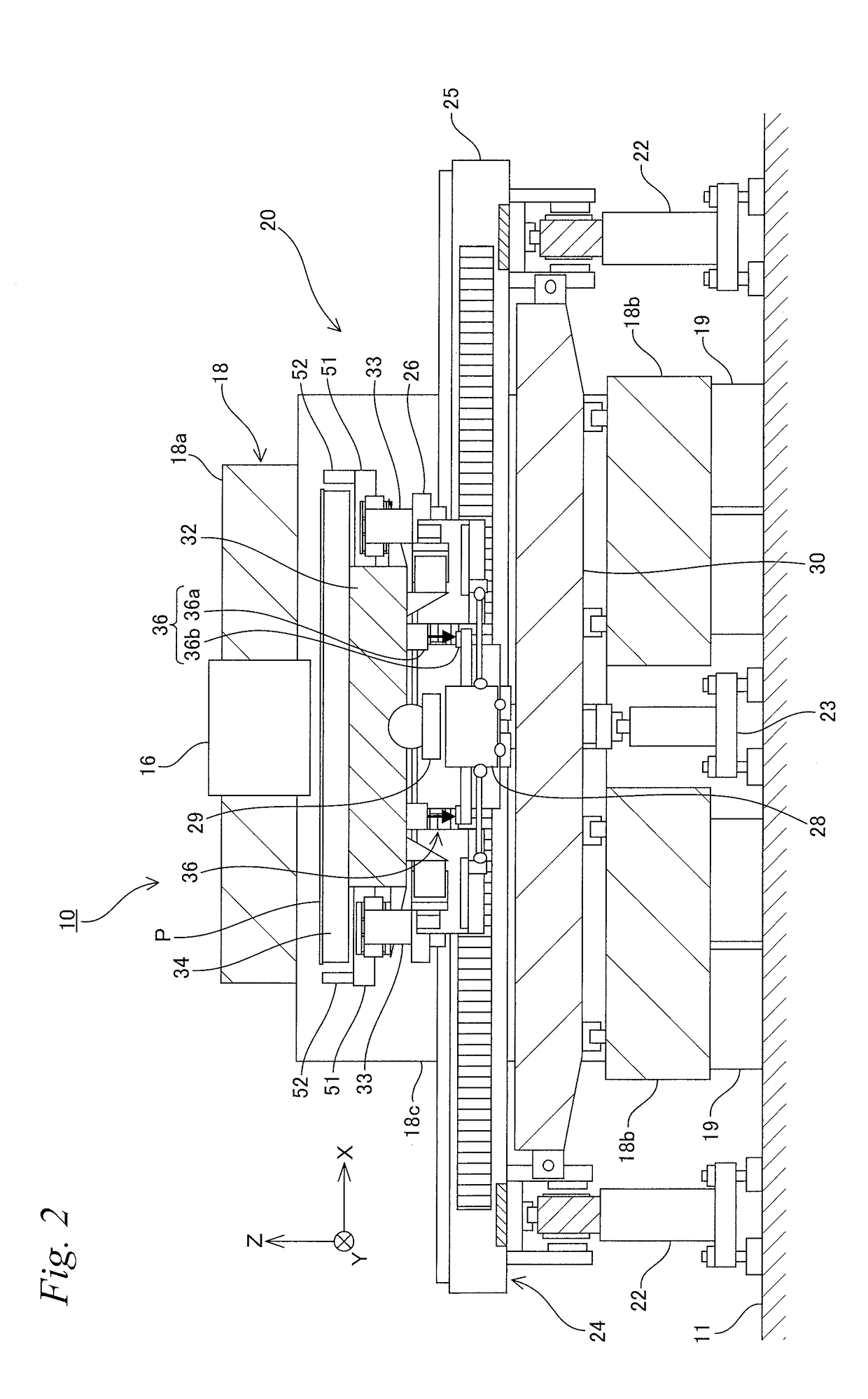
[0038]FIG. 1 schematically shows a structure of a liquid crystal exposure apparatus 10 according to the first embodiment. Liquid crystal exposure apparatus 10 is a projection exposure apparatus of a step-and-scan method, or a so-called scanner whose exposure target is a rectangular (square-shaped) glass substrate P (hereinafter simply referred to as substrate P) used in, for example, a liquid crystal display device (flat panel display) or the like.

[0039]Liquid crystal exposure apparatus 10 has an illumination system 12, a mask stage device 14 that holds a mask M on which a circuit pattern and the like is formed, a projection optical system 16, an apparatus main section 18, a substrate stage device 20 that holds substrate P whose surface (a surface facing a +Z side in FIG. 1) is coated with a resist (sensitive agent), a control system for these parts and the like. In the description below, a direction in wh...

second embodiment

[0105]Next, a second embodiment will be described, based on FIGS. 17 to 20C. Since the structure of the liquid crystal exposure apparatus according to the second embodiment is the same as the first embodiment previously described except for the structure of a part of substrate encoder system 50, only the different points will be described below, and for elements having the same structure and function as the first embodiment will have the same reference code as the first embodiment and the description thereabout will be omitted.

[0106]FIG. 17 shows substrate holder 34 and the pair of head units 60 of substrate encoder system 50 according to the second embodiment in a planar view, along with projection optical system 16. In FIG. 17, to make the description comprehensive, illustration of encoder base 54 and the like is omitted. Also, in FIG. 17, along with head unit 60 (Y slide table 62) illustrated in a dotted line, illustration of X head 64x and Y head 64y provided on the upper surfac...

third embodiment

[0232]Next, a third embodiment will be described, based on FIG. 21. Since the structure of the liquid crystal exposure apparatus according to the third embodiment is the same as the first and the second embodiments previously described except for the structure of apart of substrate encoder system 50, only the different points will be described below, and for elements having the same structure and function as the first and the second embodiments will have the same reference code as the first and the second embodiments, and the description thereabout will be omitted.

[0233]FIG. 21 shows substrate holder 34 and the pair of head units 60 of substrate encoder system. 50 according to the third embodiment in a planar view, along with projection optical system 16. In FIG. 21, to make the description comprehensive, illustration of encoder base 54 and the like is omitted. Also, in FIG. 21, along with head unit 60 (Y slide table 62) illustrated in a dotted line, illustration of X head 64x and Y...


PUM

PropertyMeasurementUnit
diagonal lengthaaaaaaaaaa
wavelengthaaaaaaaaaa

Abstract

A control system controls a drive system of a substrate holder, based on correction information to compensate for measurement error of a measurement system including an encoder system that occurs due to movement of at least one of a plurality of grating areas (scale), a plurality of heads and a substrate holder, and position information measured by the measurement system, and a measurement beam from a head of each of the plurality of heads moves off from one of the plurality of grating areas and switches to another adjacent grating area, during the movement of the substrate holder in the X-axis direction.

Description

TECHNICAL FIELD[0001]The present invention relates to exposure apparatuses and exposure methods, and flat panel display manufacturing methods, and more particularly, to an exposure apparatus and an exposure method used in a lithography process for producing micro-devices such as a liquid crystal display device, and a flat panel display manufacturing method using the exposure apparatus and the exposure method.BACKGROUND ART[0002]Conventionally, in a lithography process for producing electronic devices (micro-devices) such as a liquid crystal display device or a semiconductor device (such as an integrated circuit), exposure apparatuses are used such as an exposure apparatus of a step-and-scan method (a so-called scanning stepper (also called a scanner)) that transfers a pattern formed on a mask irradiated with an energy beam, while a mask (photomask) or a reticle (hereinafter collectively called a “mask”) and a glass plate or a wafer (hereinafter collectively called a “substrate”) are...

Claims


Application Information

Patent Timeline
Patent Type & Authority Applications(United States)
IPC IPC(8): G03F7/20G02F1/13
CPCG03F7/70133G02F1/1303G03F7/70775G03F7/7085G03F7/70725G03F9/7049G03F7/2057G03F7/7055G03F7/706G03F7/70258G03F7/70308G03F7/70141G03F7/20
Inventor SHIRATO, AKINORISHIBUYA, TAKASHI
Owner NIKON CORP
Why Eureka
Try Eureka