Semiconductor memory device

a memory device and semiconductor technology, applied in the field of semiconductor memory devices, can solve the problems of data loss, damage to data of memory cells coupled to word lines adjacent to frequently activated word lines, and the amount of charges stored in the capacitor, so as to achieve efficient preventing row hammering and improve the operation reliability according to burst refresh mode

Active Publication Date: 2018-10-11
SK HYNIX INC
View PDF2 Cites 69 Cited by
  • Summary
  • Abstract
  • Description
  • Claims
  • Application Information

AI Technical Summary

Benefits of technology

[0040]In the embodiments, by efficiently preventing row hammering in a burst ref...

Problems solved by technology

However, data may be lost because an initial amount of charges stored in the capacitor may decrease due to leakage current attributable to the PN junction of a MOS transistor, or the like.
In this regard, as a coupling effect between adjacent word lines increases as described above, a phenomenon occurs, in which the data of a memory cell coupled to a word line adjacent to a frequently activated word...

Method used


Image

  • Semiconductor memory device
  • Semiconductor memory device
  • Semiconductor memory device

Examples


first embodiment

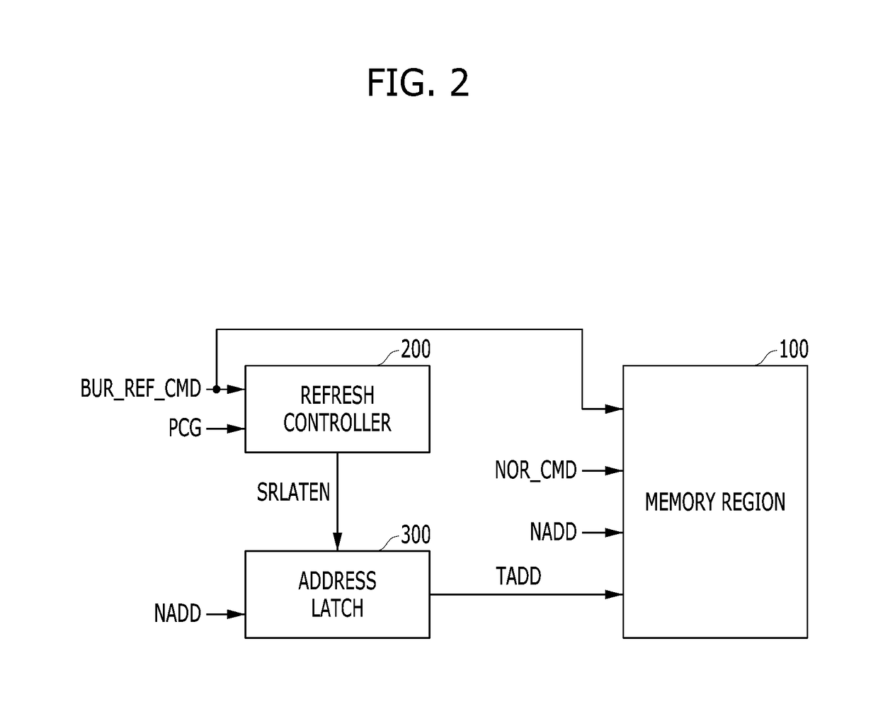
[0055]FIG. 2 is a block diagram illustrating a semiconductor memory device in accordance with the present invention.

[0056]Referring to FIG. 2, the semiconductor memory device may include a memory region 100, a refresh controller 200 and an address latch 300.

[0057]The memory region 100 may perform a normal operation based on a normal command signal NOR_CMD and a normal address signal NADD, and perform a target refresh operation based on a burst refresh command signal BUR_REF_CMD and a target address signal TADD. While not shown in the drawing, the memory region 100 may include a memory array having a plurality of memory cells arranged in a row direction and a column direction and peripheral circuits for performing the normal operation and the target refresh operation. For example, the peripheral circuits may include a row decoder and a word line driver for controlling the memory array by row.

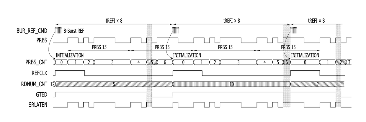
[0058]The burst refresh command signal BUR_REF_CMD may include a plurality of normal refresh ...

second embodiment

[0088]FIG. 8 is a block diagram illustrating a semiconductor memory device in accordance with the present invention.

[0089]Referring to FIG. 8, the semiconductor memory device may include a memory region 1100, a refresh controller 1200 and an address latch 1300.

[0090]Since the memory region 1100 and the address latch 1300 may have substantially the same configurations as the memory region 100 and the address latch 300 illustrated in the first embodiment, descriptions for the memory region 1100 and the address latch 1300 will be omitted herein. Hereafter, the refresh controller 1200 will be described in detail.

[0091]FIG. 9 is a block diagram illustrating the refresh controller 1200 shown in FIG. 8.

[0092]Referring to FIG. 9, the refresh controller 1200 may include a count circuit 1210, a cycle guide circuit 1220, a randomization circuit 1230 and a control circuit 1240.

[0093]Since the count circuit 1210, the cycle guide circuit 1220 and the control circuit 1240 may have substantially th...


PUM


Abstract

A semiconductor memory device includes a first count circuit suitable for counting a first clock signal which continuously toggles in each burst refresh cycle, and generating a first count code signal, based on a burst refresh command signal; a cycle guide circuit suitable for generating a second clock signal which toggles once in each burst refresh cycle, based on the burst refresh command signal and a precharge signal; a second count circuit suitable for counting the second clock signal and generating a second count code signal; and a control circuit suitable for generating a latch control signal for latching a target address in each burst refresh cycle, based on the first count code signal and the second count code signal.

Description

CROSS-REFERENCE TO RELATED APPLICATION[0001]This application claims priority under 35 U.S.C. § 119 to Korean Patent Application No. 10-2017-0046754, filed on Apr. 11, 2017, in the Korean Intellectual Property Office, the disclosure of which is incorporated herein by reference in its entirety.TECHNICAL FIELD[0002]Exemplary embodiments relate to a semiconductor design technology, and more particularly, to a semiconductor memory device performing a refresh operation.DISCUSSION OF THE RELATED ART[0003]A memory cell of a semiconductor memory device is configured by a transistor serving as a switch and a capacitor storing charges (data). Data is divided into a logic high level (logic 1) or a logic low (logic 0) level depending on whether or not charges are present in the capacitor of the memory cell, that is, whether a voltage across the capacitor is high or low. In principle, the storage of data does not consume power because it is implemented in such a manner that charges are accumulate...

Claims


Application Information

Patent Timeline
IPC IPC(8): G11C11/406G11C11/408
CPCG11C11/40611G11C11/40603G11C11/408G11C11/406G11C11/4082
Inventor LEE, JAE-SEUNGJOO, NO-GEUN
Owner SK HYNIX INC
Why Eureka
Try Eureka