Semiconductor processing device equipped with process chamber

Active Publication Date: 2018-10-11
ALLIED TECHFINDERS +1
View PDF2 Cites 2 Cited by
  • Summary
  • Abstract
  • Description
  • Claims
  • Application Information

AI Technical Summary

Benefits of technology

[0027]With the gas supply module and the vacuum module left as they are, the entire process chamber can be easily replaced with another process chamber.
[0028]A first chamber portion with the vacuum module is fixed, and a second chamber portion and the chuck unit are replaced together or respectively such that the existing process chamber is easily modified into another processing device.
[0029]The present invention achieves standardization since it is possible to modify the processing device into an

Problems solved by technology

Even if the same process is performed, the device has a different structure depending on the device manufacturer, and even devices of the same manufacturer are not standardized.
Although Semiconductor Equipment and Materials International has created SEM

Method used


Image

  • Semiconductor processing device equipped with process chamber
  • Semiconductor processing device equipped with process chamber
  • Semiconductor processing device equipped with process chamber

Examples


Example

[0039]Hereinbelow, exemplary embodiments of the present invention will be described in detail with reference to the accompanying drawings. In these drawings, the shapes and sizes of members may be exaggerated for explicit and convenient description. In addition, the terms particularly defined considering functions and operations of the present invention may vary according to intentions or practices of users or operators. Accordingly, the definitions of the terms will be given based on the content throughout the specification.

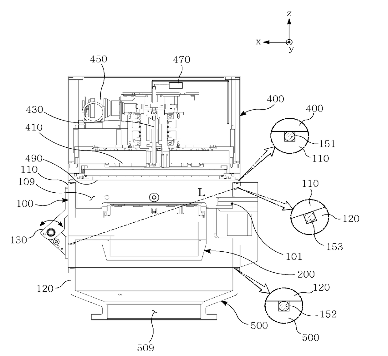
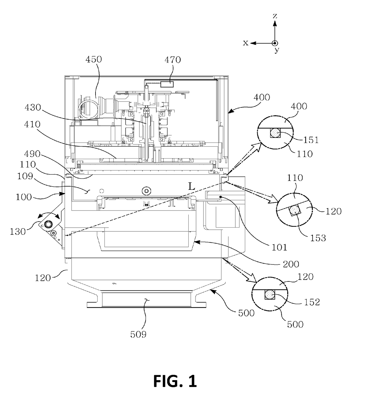
[0040]FIG. 1 is a schematic front view showing a semiconductor processing device of the present invention.

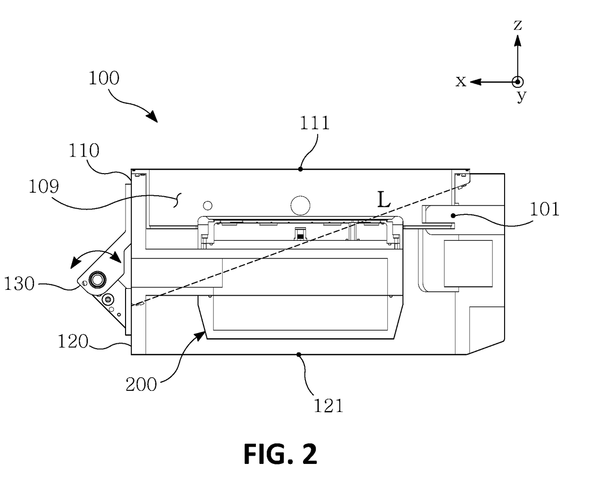
[0041]The semiconductor processing device of the present invention includes a process chamber 100 and a chuck unit 200.

[0042]The chuck unit 200 is disposed in an inner space 109 of the process chamber 100. The chuck unit 200 supports a substrate processed by plasma.

[0043]The inner space 109 is provided with an upper opening portion 111 on an upper side there...


PUM


Abstract

A semiconductor processing device according to the present invention includes a process chamber having an inner space in which plasma is generated and a chuck unit disposed in the inner space and supporting a substrate processed by the plasma. The process chamber includes a first chamber portion and a second chamber portion that are opened from each other, and when the first chamber portion and the second chamber portion are closed together, the process chamber is provided with the inner space in which the plasma is generated. When the first chamber portion and the second chamber portion are opened from each other, the chuck unit is exposed to outside.

Description

CROSS REFERENCE TO RELATED APPLICATION[0001]The present application claims priority to Korean Patent Application NO. 10-2017-0041458, filed Mar. 31, 2017, the entire contents of which is incorporated herein for all purposes by this reference.BACKGROUND OF THE INVENTIONField of the Invention[0002]The present invention relates generally to a semiconductor processing device equipped with a standardized process chamber having a vacuum chamber in which a semiconductor substrate such as a wafer is processed.Description of the Related Art[0003]A semiconductor processing device for a surface treatment for forming a fine pattern on the surface of a semiconductor wafer includes a photolithography device that forms a pattern designed on a mask, an etching device that removes a patterned thin film on the wafer, and a deposition device that deposits a pattern thin film on the wafer.[0004]Even though the process steps are different, semiconductor processing devices have common features such as a ...

Claims


Application Information

Patent Timeline
IPC IPC(8): H01L21/67H01J37/32
CPCH01L21/67069H01J37/32715H01J37/32458H01J37/32743H01J37/32899H01J2237/334H01L21/6719H01L21/67126H01L21/3065H01L21/67184H01L21/67739H01L21/67742H01L21/67772H01L21/683
Inventor SUH, KEE WON
Owner ALLIED TECHFINDERS
Why Eureka
Try Eureka