
Semiconductor memory device and operating method thereof

a memory device and semiconductor technology, applied in the field of semiconductor memory devices, can solve problems such as data loss and decrease of charges that are stored in capacitors

Active Publication Date: 2018-10-18
SK HYNIX INC
View PDF0 Cites 0 Cited by
  • Summary
  • Abstract
  • Description
  • Claims
  • Application Information

AI Technical Summary

Benefits of technology

This solution minimizes the influence of transistor mismatches, optimizing the bit-line sense amplifier's performance and extending data retention time, thereby reducing the frequency and current consumption of refresh operations.

Problems solved by technology

However, since current leaks due to a PN junction of a transistor, the initial amount of charges that are stored in a capacitor may decrease, thereby causing data loss.

Method used


Image

  • Semiconductor memory device and operating method thereof
  • Semiconductor memory device and operating method thereof
  • Semiconductor memory device and operating method thereof

Examples


Embodiment Construction

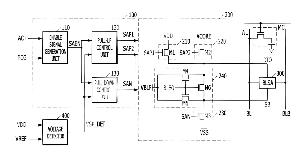
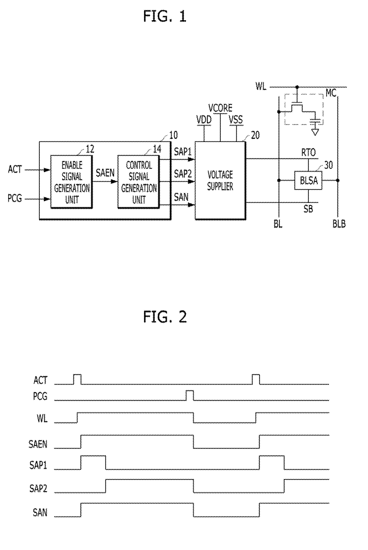
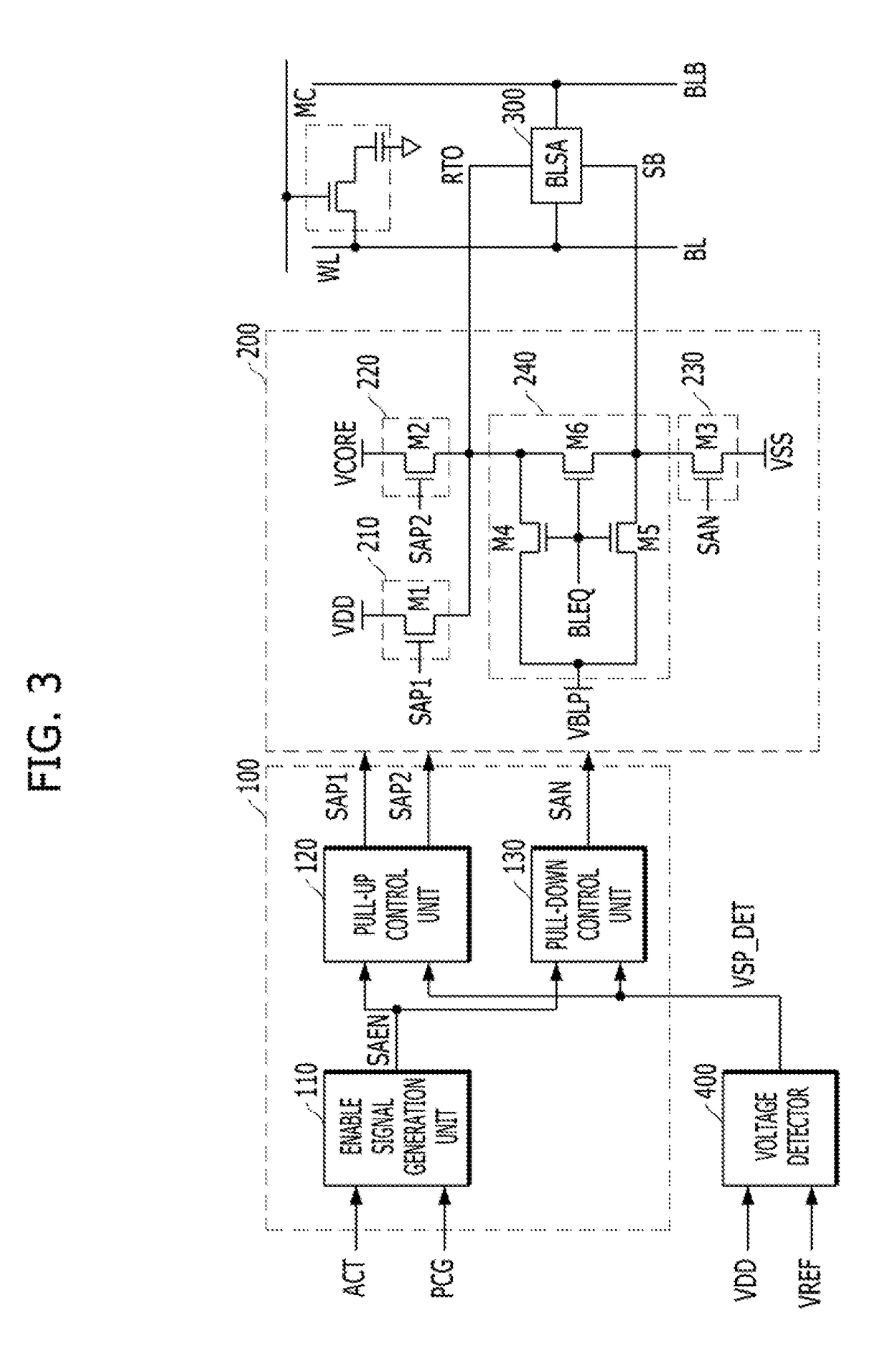
[0021]Exemplary embodiments of the present invention will be described below in more detail with reference to the accompanying drawings. The present invention may, however, be embodied in different forms and should not be construed as limited to the embodiments set forth herein. Rather, these embodiments are provided so that this disclosure will be thorough and complete, and will fully convey the scope of the present invention to those skilled in the art. Throughout the disclosure, like reference numerals refer to like parts throughout the various figures and embodiments of the present invention.

[0022]It will be understood that, although the terms “first”, “second”, “third”, and so on may be used herein to describe various elements, these elements are not limited by these terms. These terms are used to distinguish one element from another element. Thus, a first element described below could also be termed as a second or third element without departing from the spirit and scope of th...


PUM


Abstract

A semiconductor memory device may include a sense amplifier for sensing and amplifying data of a bit line pair with pull-up and pull-down driving voltages; a voltage supplier for supplying a power supply voltage or an internal voltage lower than the power supply voltage as the pull-up driving voltage through a pull-up power supply line in response to a first or second pull-up control signal, and supplying a ground voltage as the pull-down driving voltage through a pull-down power supply line in response to a pull-down control signal; a voltage detector for detecting a voltage level of the power supply voltage and outputting a detection signal; and a control signal generator for generating the first and second pull-up control signals, and the pull-down control signal and delaying an enabling timing of one of the first pull-up and pull-down control signals in response to the detection signal.

Description

CROSS-REFERENCE TO RELATED APPLICATIONS[0001]The present application claims priority under 35 U.SC. 119(a) to Korean Patent Application No. 10-2016-0108279, filed on Aug. 25, 2016, which is incorporated herein by reference in its entirety.BACKGROUND1. Field[0002]Exemplary embodiments of the present invention relate to a semiconductor design technology, and more particularly, to a semiconductor memory device capable of performing a refresh operation.2. Description of the Related Art[0003]A semiconductor memory device, such as a dynamic random access memory (DRAM), generally includes a plurality of memory cells. Each memory cell may typically include a transistor that serves as a switch and a capacitor that stores charges, that is, data. A memory cell is determined to have stored data in a logic ‘high’ level (a logic value of ‘1’) or a logic ‘low’ level (a logic value of ‘0’) based on whether there are charges in a capacitor thereof, that is, whether the terminal voltage of the capaci...

Claims


Application Information

Patent Timeline
Patent Type & Authority Applications(United States)
IPC IPC(8): G11C11/4094G11C11/4091G11C11/4076G11C11/4074G11C11/406G11C5/14G11C7/08G11C8/08G11C8/10G11C8/12
CPCG11C11/40611G11C7/08G11C5/143G11C8/10G11C8/12G11C11/406G11C11/4076G11C11/4091G11C8/08G11C11/4094G11C11/4074Y02D10/00
Inventor JO, MI-HYEON
Owner SK HYNIX INC
Features
  • Generate Ideas
  • Intellectual Property
  • Life Sciences
  • Materials
  • Tech Scout
  • Unparalleled Data Quality
  • Higher Quality Content
  • 60% Fewer Hallucinations
Learn More