
Semiconductor device and projection-type display unit

a technology of semiconductor devices and display units, applied in semiconductor devices, identification means, instruments, etc., can solve the problems of easy occurrence of film detachment and low light-shielding performance, and achieve enhanced light-shielding performance, enhanced light-shielding performance for the ldd region, and suppression of image deficiency of liquid crystal panels.

Active Publication Date: 2018-11-15
SONY CORP
View PDF1 Cites 0 Cited by
  • Summary
  • Abstract
  • Description
  • Claims
  • Application Information

AI Technical Summary

Benefits of technology

This patent is about a semiconductor device and a projection-type display unit that improve light-shielding and resistance to film detachment. The device includes a gate electrode that is made up of two electroconductive films, with the second film extending from the side of the semiconductor layer to the bottom face of each opening that interposes the semiconductor layer. This increases the adhesiveness between the gate electrode and the gate insulating layer, as well as the light-shielding property of the semiconductor layer. This enhances the performance and durability of the semiconductor device.

Problems solved by technology

However, structures disclosed in the above-described PTL 1 to PTL 3 have issues such as a low light-shielding performance for light incident from a side into a LDD region, and easy occurrence of film detachment due to low adhesiveness between an insulating film and an electroconductive film as well as a stress difference between films.

Method used


Image

  • Semiconductor device and projection-type display unit
  • Semiconductor device and projection-type display unit
  • Semiconductor device and projection-type display unit

Examples


first embodiment (

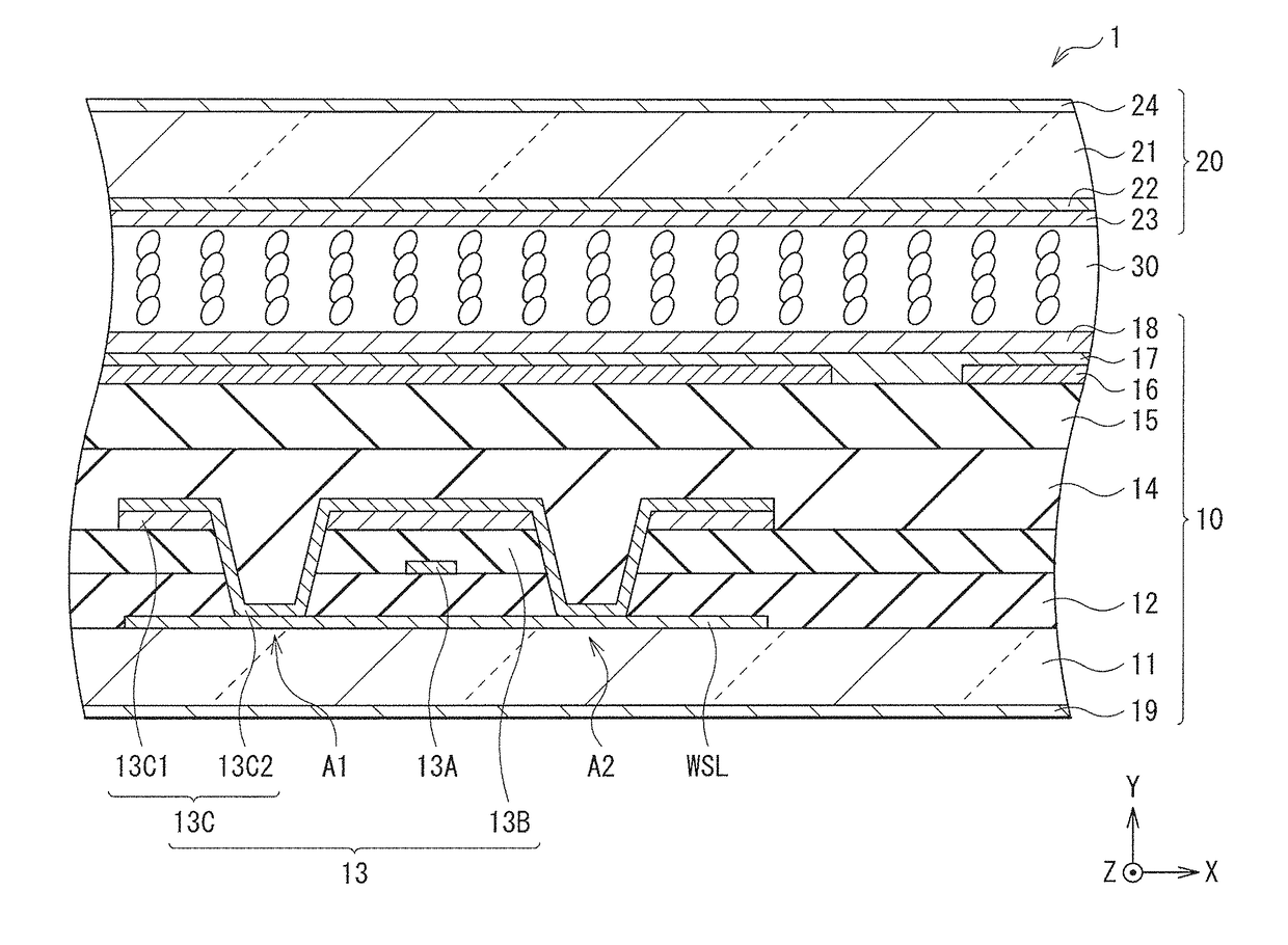
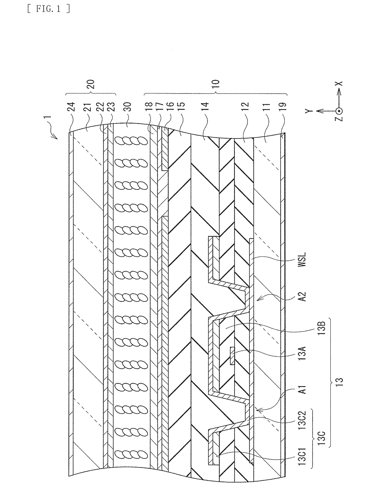
1. First Embodiment (an example of a liquid crystal projection-type display unit in which a gate electrode includes a first electroconductive film and a second electroconductive film having a light-shielding property, and the second electroconductive film extends to a bottom face of a coupling aperture for a scanning line)

[0028]1-1. Configuration of Liquid Crystal Panel

[0029]1-2. Overall Configuration of Projection-Type Display Unit

[0030]1-3. Workings and Effects

second embodiment (

2. Second Embodiment (an example in which an electrically floating light-shielding film is further provided above the gate electrode)

3. Modification Example (an example in which a second electroconductive film is formed as a laminated film)

4. Examples

first embodiment

1. First Embodiment

[0031]FIG. 1 illustrates a cross-sectional configuration of a liquid crystal panel 1 included in a projection-type display unit (a projector 100, see FIG. 4) according to a first embodiment of the disclosure. The projector 100 includes, for example, components such as the liquid crystal panel 1 illustrated in FIG. 1, and a drive circuit 40 including a display control section 41, a data driver 42, and a gate driver 43, and displays an image on a screen 200 on the basis of a picture signal Din inputted from outside (for each of the components, see FIG. 4 and FIG. 5).

(1-1. Configuration of Liquid Crystal Panel)

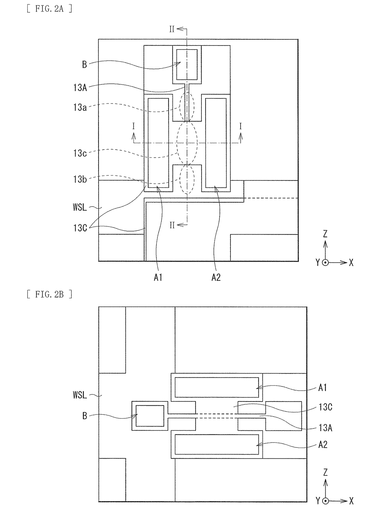
[0032]FIG. 2A illustrates a planar configuration of the liquid crystal panel 1 illustrated in FIG. 1, and FIG. 1 is a cross-sectional view corresponding to a line I-I in FIG. 2. FIG. 3 illustrates a cross-sectional configuration along a line II-II in FIG. 2A. In the liquid crystal panel 1, a liquid crystal layer 30 is sealed between a drive substrate 10 and a c...


PUM

PropertyMeasurementUnit
thicknessaaaaaaaaaa
thicknessaaaaaaaaaa
thicknessaaaaaaaaaa

Abstract

A semiconductor device according to an embodiment of the disclosure includes: a first substrate; a TFT element provided on the first substrate with a first interlayer insulating layer interposed therebetween, and including a semiconductor layer and a gate electrode that is provided on the semiconductor layer with a gate insulating layer interposed therebetween; and a second substrate disposed to face the first substrate. The gate electrode includes a first electroconductive film and a second electroconductive film that has a light-shielding property in order from side of the semiconductor layer. The second electroconductive film extends from a side face to a bottom face of each of a pair of openings that are provided to interpose the semiconductor layer.

Description

TECHNICAL FIELD[0001]The disclosure relates to a semiconductor device including a light-shielding film on a semiconductor layer, and a projection-type display unit including the semiconductor device.BACKGROUND ART[0002]In recent years, a projection-type liquid crystal display (LCD: Liquid Crystal Display) that projects an image onto a screen has been widely used not only at office but also at home. The projection-type liquid crystal display (a projector) generates image light by modulating light from a light source by using a light valve, and performs display by projecting the image light onto a screen. The light valve includes a liquid crystal panel, and light is modulated by, for example, active matrix driving of each pixel depending on a picture signal from outside. For this reason, improvement of image deficiency (such as flicker and display unevenness) of the liquid crystal panel is desired.[0003]To suppress occurrence of the image deficiency of the liquid crystal panel, it is ...

Claims


Application Information

Patent Timeline
Patent Type & Authority Applications(United States)
IPC IPC(8): G02F1/1362H01L29/786G02F1/1368
CPCG02F1/136209H01L29/78621G02F1/1368H01L29/78633H01L27/124G09F9/30
Inventor ABE, KAZUKIINAGE, SHINYAODA, NOBUHIKOKAIDA, MASAHIRONAGURA, MORIYASU
Owner SONY CORP
Learn More