
Electro-optical device and electronic apparatus

a technology of electrooptical devices and electronic devices, applied in non-linear optics, identification means, instruments, etc., can solve the problems of reducing the quality of display images, insufficient shielding, and light obliquely applied between shielding films and channel regions, so as to inhibit the generation of light leakage current, increase light shielding performance, and achieve high-quality images without flicker

Inactive Publication Date: 2006-10-17
138 EAST LCD ADVANCEMENTS LTD
View PDF15 Cites 8 Cited by
  • Summary
  • Abstract
  • Description
  • Claims
  • Application Information

AI Technical Summary

Benefits of technology

"The present invention provides an electro-optical device that prevents the generation of light leakage current by improving the light-shielding performance of thin film transistors. This is achieved by using a shielding layer between data lines and pixel electrodes. The shielding layer can be formed of a multi-layered film containing a low resistance film, which increases the electric conductivity and reduces the size of capacitor lines without special restrictions. The capacitor line can also be formed of another material to implement a light-shielding function to shield the thin film transistor from light. The multi-layered film can provide various functions such as a fixed potential capacitor electrode, a light-absorbing material, and a conductive material for setting the first electrode of a storage capacitor. The flexibility to design the electro-optical device can also be enhanced by using the multi-layered film for the capacitor line."

Problems solved by technology

However, the following problems are presented by the above-described related art light-shielding techniques.
Thus, light obliquely applied between the shielding film and the channel region cannot be sufficiently shielded.
Therefore, insufficient shielding for the obliquely incident light presents a problem in a practical sense.
Accordingly, it becomes more difficult to provide sufficient light-shielding by the above-described related art light-shielding techniques, and thus, flickering occurs due to a change in the TFT transistor characteristics, thereby reducing the quality of display images.
If such an area is increased, however, it is difficult to respond to demands for increasing the aperture ratio of each pixel for enhancing the brightness of display images.
In view of this point, an increased area in which the light-shielding film is formed disadvantageously intensifies the internal-surface reflection light or the multiple reflection light.

Method used


Image

  • Electro-optical device and electronic apparatus
  • Electro-optical device and electronic apparatus
  • Electro-optical device and electronic apparatus

Examples


first exemplary embodiment

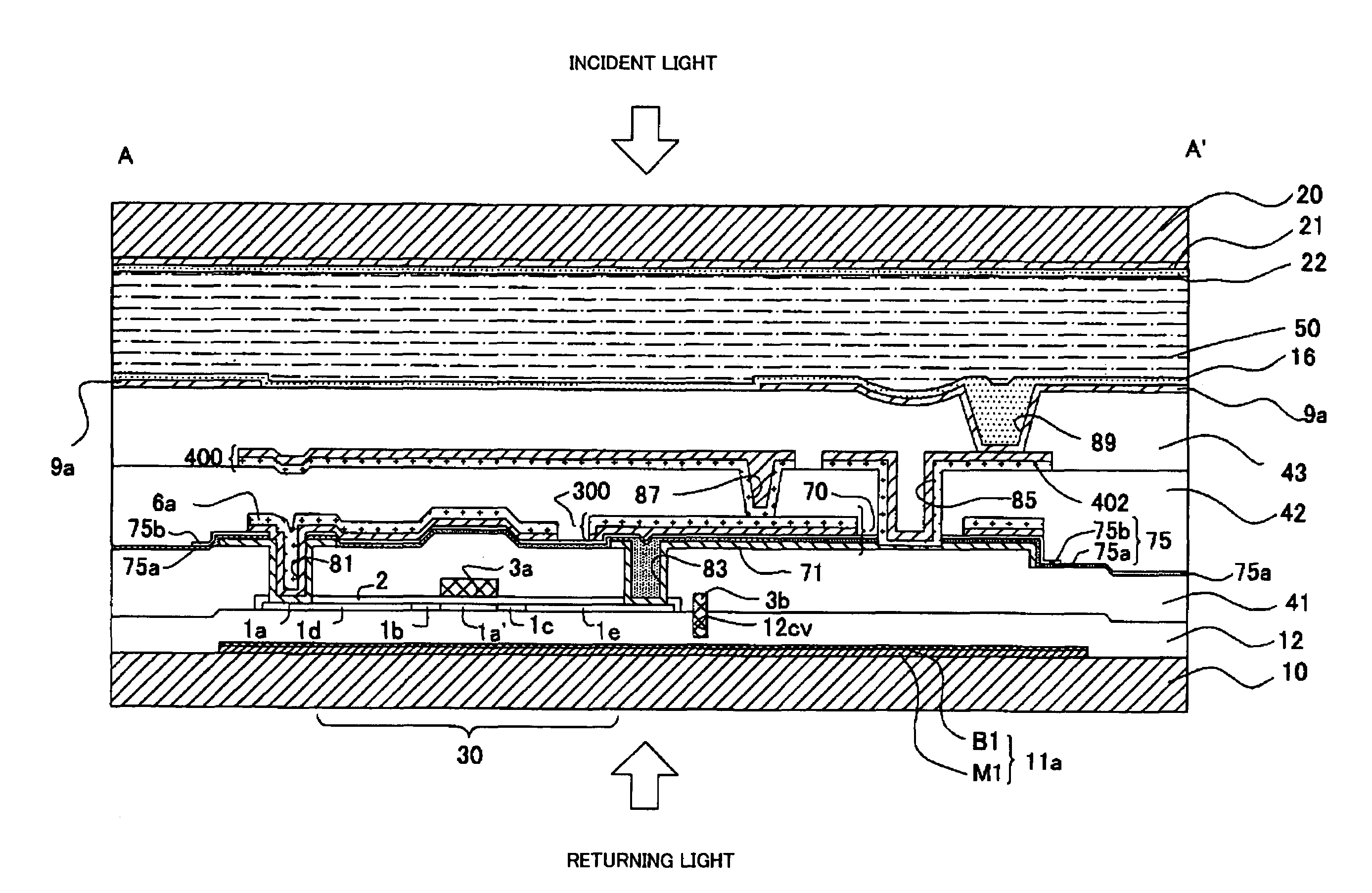
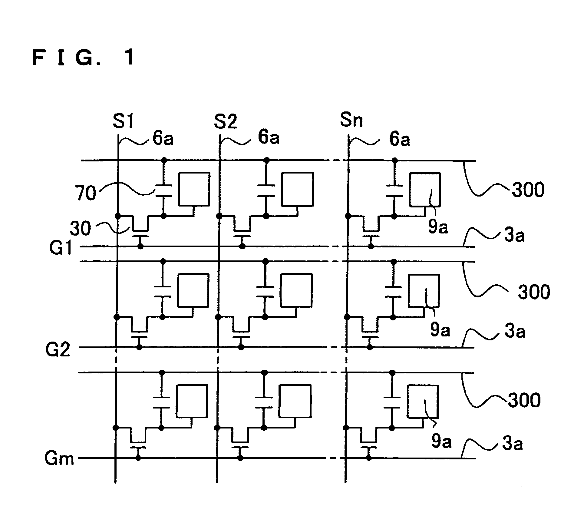
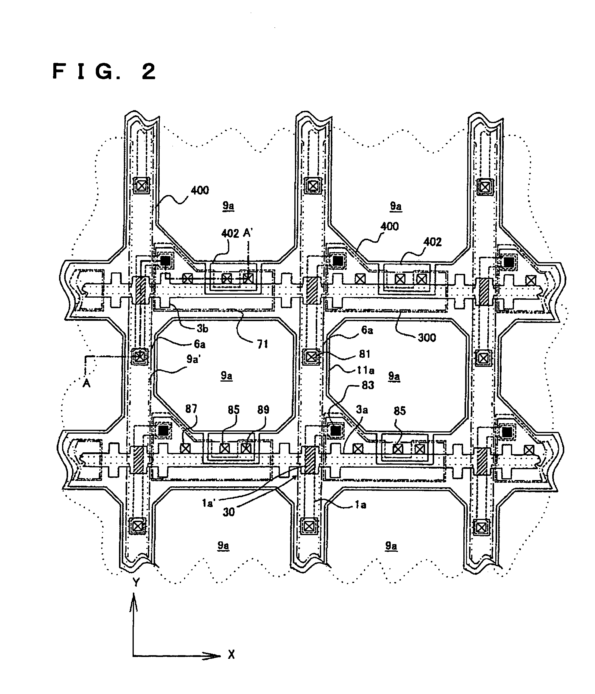
[0111]The configuration of a pixel portion of an electro-optical device according to a first exemplary embodiment is described below with reference to FIGS. 1 through 4. FIG. 1 illustrates an equivalent circuit of various elements, wiring patterns, etc., in a plurality of pixels formed in a matrix, which forms an image display area of the electro-optical device. FIG. 2 is a plan view illustrating a plurality of pixel groups disposed adjacent to each other having data lines, scanning lines, pixel electrodes, etc. thereon on a TFT array substrate. FIG. 3 is a plan view illustrating the essential portion extracted from the pixel groups shown in FIG. 2, in order to show the positional relationship among the data lines, the shielding layer, and the pixel electrodes. FIG. 4 is a sectional view taken along plane A–A′ of FIG. 2. In FIG. 4, the scales of the individual layers and the individual elements are different in order to easily identify the sizes of the layers and elements.

[0112]In F...


PUM

PropertyMeasurementUnit
thicknessaaaaaaaaaa
dielectric constantaaaaaaaaaa
thicknessaaaaaaaaaa

Abstract

An electro-optical device includes: data lines extending in a first direction on a substrate; scanning lines extending in a second direction and intersecting with the data lines; pixel electrodes and thin film transistors disposed corresponding to intersections of the data lines and the scanning lines; storage capacitors electrically connected to the thin film transistors and the pixel electrodes; and a shielding layer disposed between the data lines and the pixel electrodes. One of a pair of electrodes forming the storage capacitor is formed of a multi-layered film containing a low resistance film.

Description

BACKGROUND OF THE INVENTION[0001]1. Field of Invention[0002]The present invention relates to active-matrix-driven electro-optical devices. More particularly, the invention relates to an electro-optical device in which thin film transistors (hereinafter sometimes referred to as “TFTs”) for switching pixels are provided in a laminated structure on a substrate. The invention also relates to a manufacturing method for such an electro-optical device and to an electronic apparatus provided with the electro-optical device as a light valve. The invention also pertains to electrophoretic devices for, for example, electronic paper, EL (electroluminescent) devices, and devices using electron emission elements (field emission display and surface-conduction electron-emitter display).[0003]2. Description of Related Art[0004]In a TFT-active-matrix-driven electro-optical device, when light is incident on a channel region of a pixel-switching TFT provided for each pixel, a light leakage current is g...

Claims


Application Information

Patent Timeline
Patent Type & Authority Patents(United States)
IPC IPC(8): H01L29/04G02F1/1335G02F1/1362G02F1/1368G09F9/30H01L21/77H01L27/12H01L27/13H01L29/786
CPCG02F1/136213H01L27/1255G02F1/136227G02F1/136209H01L27/124G02F1/136286G02F1/1335
Inventor YAMASAKI, YASUJITAKAHARA, KENICHIIKI, TAKUNORI
Owner 138 EAST LCD ADVANCEMENTS LTD
Learn More