Output driving circuit

Active Publication Date: 2018-11-29
SK HYNIX INC
View PDF2 Cites 1 Cited by
  • Summary
  • Abstract
  • Description
  • Claims
  • Application Information

AI Technical Summary

Benefits of technology

This patent is about an improved output driving circuit for a semiconductor device that can operate effectively across a greater range of voltages and exhibits enhanced reliability. The circuit includes a pull-down driver, an input / output control logic, a gate control logic, and an inverter. The pull-down driver has three transistors connected between a pad and ground, and the input / output control logic controls the transistors to transfer a first control signal to the third transistor. The gate control logic controls the transistors to output a feedback voltage to the first transistor. The inverter inverts the enable signal and sends it to the gate control logic. This circuit design allows for better reliability and performance of the semiconductor device.

Problems solved by technology

However, an IO circuit manufactured using CMOSFETs having a medium gate oxide for 1.8 V operation or a thin gate oxide for 0.9 V operation may not work properly when a voltage of 3.3 V is applied.

Method used


Image

  • Output driving circuit
  • Output driving circuit
  • Output driving circuit

Examples


Embodiment Construction

[0045]Embodiments of the present disclosure are described with reference to the accompanying drawings in order to describe the present disclosure in detail so that those having ordinary knowledge in the technical field to which the present disclosure pertains can easily practice the present disclosure. It should be noted that the same reference numerals are used to designate the same or similar elements throughout the drawings. In the following description of the present disclosure, detailed descriptions of known functions and configurations which are deemed to make the gist of the present disclosure obscure will be omitted.

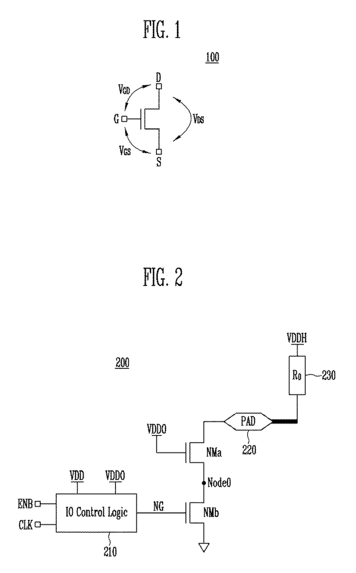
[0046]FIG. 1 is a diagram explaining the operating condition of a medium gate oxide device.

[0047]In order for a medium gate oxide device 100 to stably operate, a gate-source voltage VGS, a gate-drain voltage VGD, and a drain-source voltage VDS of the medium gate oxide device 100 should satisfy certain reliability conditions. For example, if the medium gate oxide ...


PUM


Abstract

The output driving circuit include a pull-down driver, an input / output (IO) control logic, a gate control logic, and an inverter. The pull-down driver includes first, second, and third transistors that are sequentially coupled between a pad and a ground node. The IO control logic is configured to receive a clock signal and an enable signal, and transfer a first control signal to the third transistor. The gate control logic is configured to receive a voltage of the pad and output a feedback voltage to a gate electrode of the first transistor. The inverter is configured to invert the enable signal and transfer an inverted enable signal to the gate control logic. Therefore, the reliability of the output driving circuit can be improved.

Description

CROSS-REFERENCE TO RELATED APPLICATION[0001]The present application claims priority under 35 U.S.C. § 119(a) to Korean patent application number 10-2017-0063919 filed on May 24, 2017 In the Korean Intellectual Property Office, the entire disclosure of which is incorporated herein by reference.BACKGROUNDField of Invention[0002]Various embodiments of the present disclosure generally relate to an electronic device, and more particularly, to an output driving circuit for a semiconductor device, a semiconductor device including the output driving circuit and various electronic devices including the same.Description of Related Art[0003]In recent chips, a high-speed interface integrated processor (IP) requiring a low-supply voltage and a high-speed operation is widely used. Accordingly, CMOSFETs having a medium gate oxide for 1.8 V operation or CMOSFETs having a thin gate oxide for 0.9 V operation, rather than CMOSFETs having a thick gate oxide for 3.3 V operation, are widely used.[0004]Ho...

Claims


Application Information

Patent Timeline
IPC IPC(8): H03K19/003H03K19/00H03K19/017H03K19/177
CPCH03K19/00315H03K19/0005H03K19/01742H03K19/17788H03K19/0948
Inventor LEE, SEUNG HO
Owner SK HYNIX INC
Why Eureka
Try Eureka