Light-emitting element package and lighting device

a technology of light-emitting elements and lighting devices, which is applied in the direction of basic electric elements, semiconductor devices, electrical equipment, etc., can solve the problems of very low power consumption of light-emitting diodes, and achieve the effects of improving the stiffness of the first, improving the efficiency of the first, and improving the quality of the second

Active Publication Date: 2018-12-13
SUZHOU LEKIN SEMICON CO LTD
View PDF5 Cites 4 Cited by
  • Summary
  • Abstract
  • Description
  • Claims
  • Application Information

AI Technical Summary

Benefits of technology

[0012]That is, in an embodiment, edge portions or curved surface portions may be disposed around a spaced space of the first and second lead frames to improve injection molding defects, thereby improving productivity.
[0014]In the light emitting device package of an embodiment, by proposing a structure in which an interval around the side portions is wider by edge portions disposed around the side portions rather than a spaced interval between side portions facing first and second lead frames, injection molding can be improved in a spaced space between the first lead frame and second lead frame.
[0016]The light emitting device package of an embodiment may include edge portions having the same thickness as those of the first and fifth side portions around the exposed first and fifth side portions of the first and second lead frames to improve stiffness of the first and second lead frames. That is, in an embodiment, stiffness of the first and second lead frames may be improved by a structure of stepped portions and edge portions disposed at edges of lower surfaces of the first and second lead frames, and simultaneously, a coupling force with a body may be improved.
[0017]In an embodiment, edge portions may be disposed around the side portions facing the first and second lead frames, and thus injection molding can be improved in a spaced space between the first lead frame and second lead frame. That is, the embodiment improves the injection molding defects around the spaced apart spaces of the first and second lead frames, so that the productivity can be improved.
[0018]The light emitting device package of an embodiment may include a predetermined curvature at corners of inner side surfaces of a cavity configured to expose the first and second lead frames to improve defects such as cracks which may occur at corner regions of the cavity. That is, in an embodiment, reliability of the injection molding for coupling the body and the first and second lead frames may be improved.
[0019]In addition, in an embodiment, an interval between the inner side surfaces of the cavity and the light emitting device is uniformly maintained as a whole, thereby improving light loss at corner regions of the cavity. That is, in an embodiment, light extraction efficiency may be improved.

Problems solved by technology

Since a light emitting diode generates light by using the semiconductor devices, the light emitting diode consumes very low power as compared with incandescent lamps which generate light by heating tungsten, or fluorescent lamps which generate light by colliding ultraviolet rays generated through high pressure discharge on a phosphor.

Method used


Image

  • Light-emitting element package and lighting device
  • Light-emitting element package and lighting device
  • Light-emitting element package and lighting device

Examples


Embodiment Construction

[0033]The present embodiments may be modified into another form or may be combined with some embodiments, and the scope of the present invention is not limited to each embodiment described below.

[0034]Although the matters described in a specific embodiment are not described in other embodiments, unless otherwise stated or contradictory to the description, other embodiments may be understood in connection with the description.

[0035]For example, if features for configuration A are described in a particular embodiment and features for configuration B are described in another embodiment, although embodiments in which the configurations A and B are combined are not explicitly described, unless otherwise stated or contradictory, it should be understood that the combination belongs to the scope of rights of the present invention.

[0036]Hereinafter, embodiments of the present invention capable of realizing the above objects will be described with reference to the accompanying drawings.
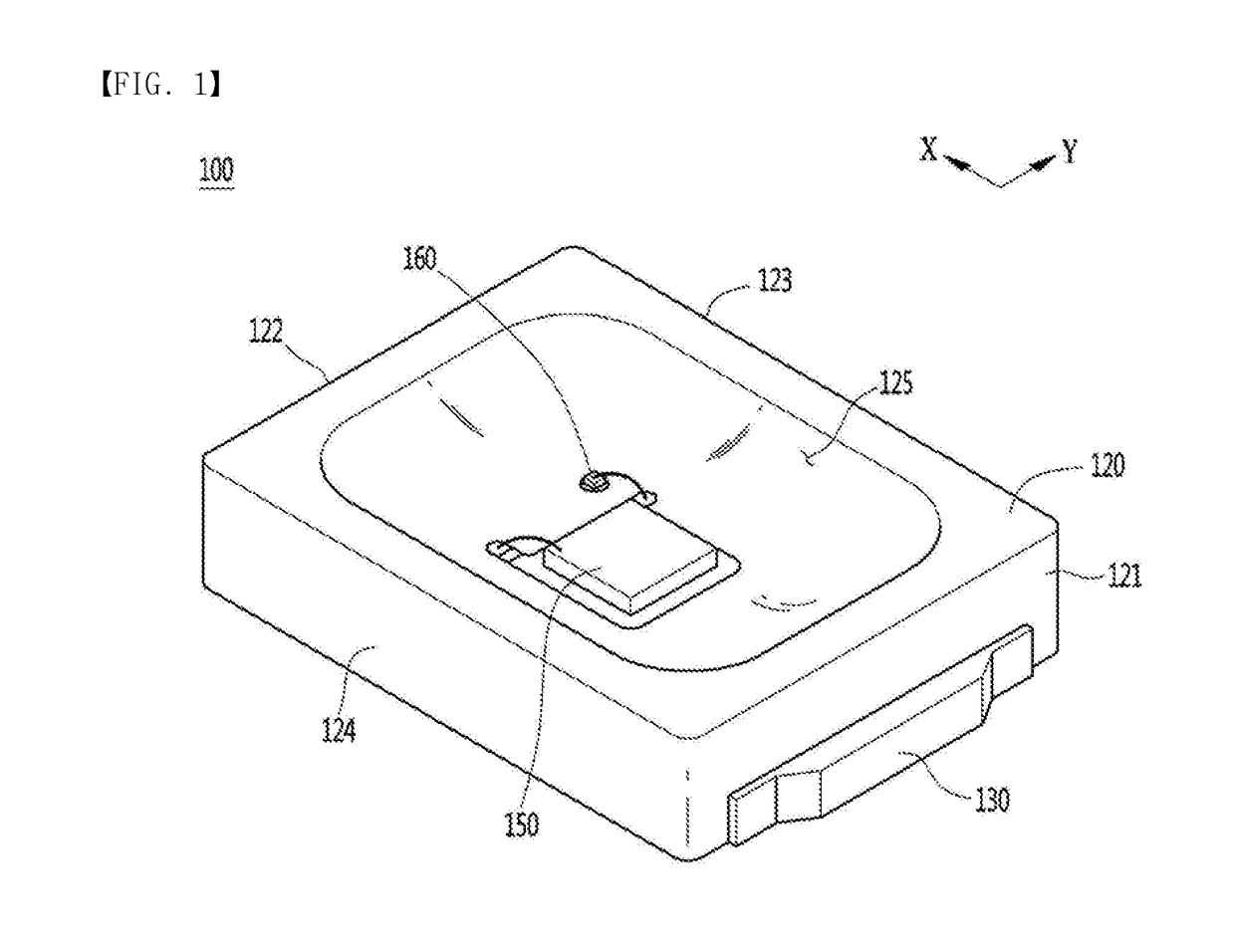
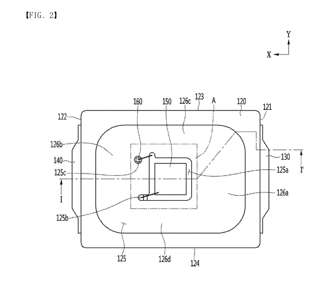
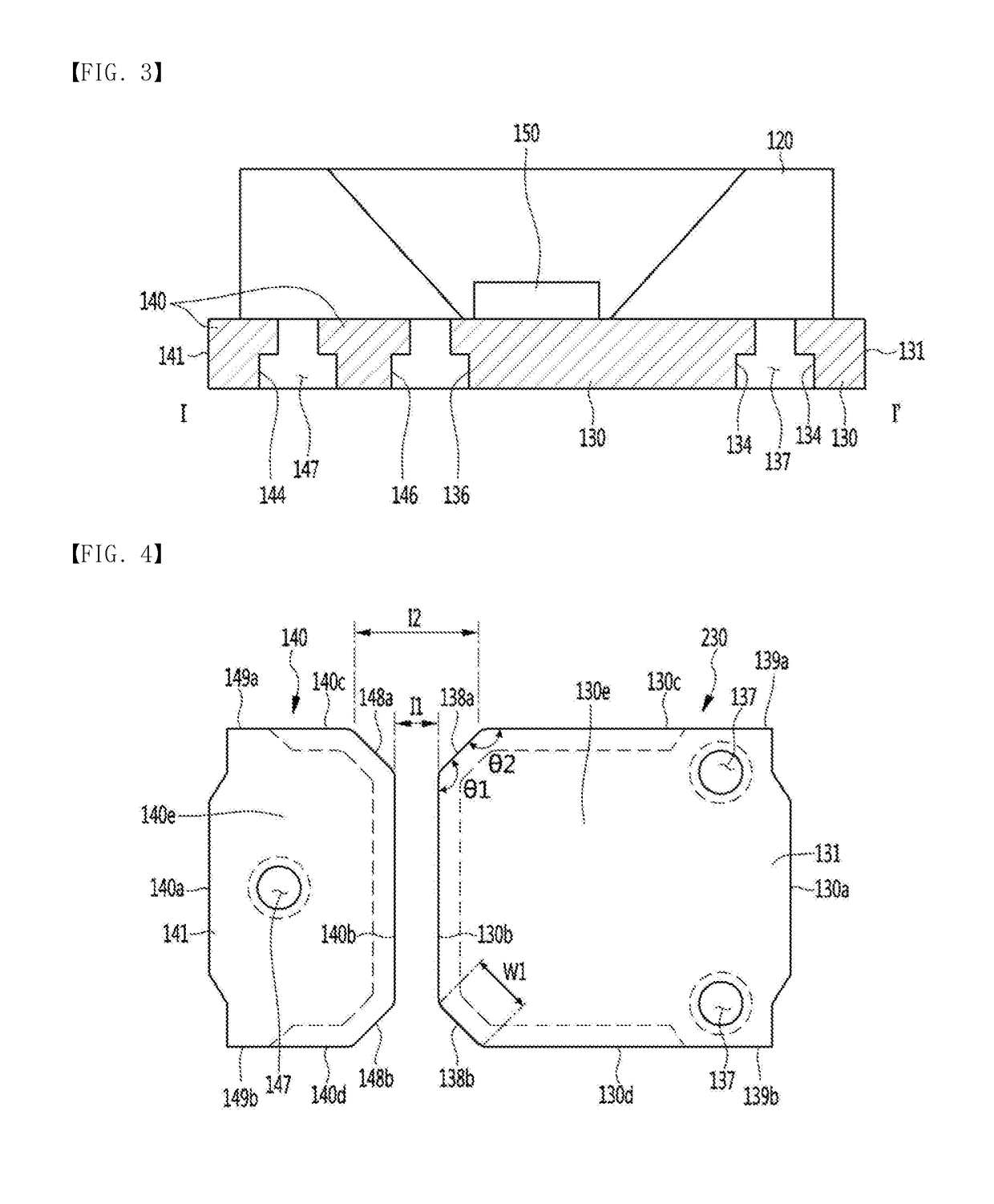
[0037]...


PUM


Abstract

Embodiments relate to a light emitting device package and a lighting device. The light emitting device package of an embodiment includes: a first lead frame; a light emitting device mounted on the first lead frame; a second lead frame spaced apart from the first lead frame in a first direction; a protective device mounted on the second lead frame; and a body coupled to the first and second lead frames, wherein the first lead frame includes a first stepped portion disposed along an edge of a lower surface thereof, and the second lead frame includes a third stepped portion disposed along an edge of a lower surface thereof, a mounting region of the protective device which is not overlapped in a vertical direction and spaced apart from the third stepped portion, and a second wire recess portion which is partially overlapped with the third stepped portion in the vertical direction, wherein the first and third stepped portions may be disposed in the body to improve injection molding into a spaced space between the first lead frame and second lead frame. That is, in an embodiment, an edge portion or a curved surface portion may be disposed around a spaced space of the first and second lead frames to improve injection molding defects, thereby improving productivity.

Description

TECHNICAL FIELD[0001]Embodiments relate to a light emitting device package and a lighting device.BACKGROUND ART[0002]A light emitting device is a kind of semiconductor devices that convert electrical energy into light, and is in the spotlight as a next generation light source replacing a conventional fluorescent lamp, an incandescent lamp, etc.[0003]Since a light emitting diode generates light by using the semiconductor devices, the light emitting diode consumes very low power as compared with incandescent lamps which generate light by heating tungsten, or fluorescent lamps which generate light by colliding ultraviolet rays generated through high pressure discharge on a phosphor.[0004]In addition, since the light emitting diode generates light using potential gaps of the semiconductor devices, the light emitting diode has long life span, fast response characteristics, and eco-friendly characteristics compared to conventional light sources.[0005]Accordingly, various studies have been...

Claims


Application Information

Patent Timeline
Patent Type & Authority Applications(United States)
IPC IPC(8): H01L33/62H01L33/32H01L33/10
CPCH01L33/62H01L33/32H01L33/10H01L25/167H01L33/405H01L33/486H01L2224/48247H01L2933/0033
Inventor YU, DONG HYUNKANG, KYUNG HOYUN, NAE SANGCHOE, MEEN SOO
Owner SUZHOU LEKIN SEMICON CO LTD
Why Eureka
Try Eureka