Circuit board for reducing transmitting loss and electronic device therewith

a technology of circuit board and transmission line, which is applied in the direction of high-frequency circuit adaptation, electric apparatus casing/cabinet/drawer, display/control unit casing, etc., can solve the problems of limiting the transmission distance of high-frequency rf signal, transmission loss, and relatively large transmission loss, so as to reduce transmission loss, reduce transmission loss, and minimize transmission loss of transmission line

Active Publication Date: 2018-12-13
SAMSUNG ELECTRONICS CO LTD
View PDF12 Cites 8 Cited by
  • Summary
  • Abstract
  • Description
  • Claims
  • Application Information

AI Technical Summary

Benefits of technology

[0006]An aspect of the present disclosure is to provide a circuit board for reducing signal transmission loss when a high frequency RF signal is transmitted in the circuit board, and an electronic device including the circuit board.
[0007]Another aspect of the present disclosure is to provide a circuit board for reducing transmission loss without a distance restriction, and an electronic device including the circuit board.
[0008]Another aspect of the present disclosure is to provide a circuit board for minimizing transmission loss of a transmission line when a signal is transmitted between external metal frames used as an antenna radiator in an RF block, and an electronic device including the circuit board.

Problems solved by technology

When a high-frequency Radio Frequency (RF) signal is transmitted in a typical printed circuit board, a transmission loss occurs due to a physical property of the printed circuit board, thereby limiting a distance for transmitting the high-frequency RF signal.
For example, the transmission loss may be caused by a conductor and / or a dielectric material of the printed circuit board.
In such a conventional printed circuit board, there is a problem in that a transmission loss is relatively great in comparison with a coaxial cable, when the transmission line for transmitting a high frequency RF signal is longer than a specific distance.

Method used


Image

  • Circuit board for reducing transmitting loss and electronic device therewith
  • Circuit board for reducing transmitting loss and electronic device therewith
  • Circuit board for reducing transmitting loss and electronic device therewith

Examples


Embodiment Construction

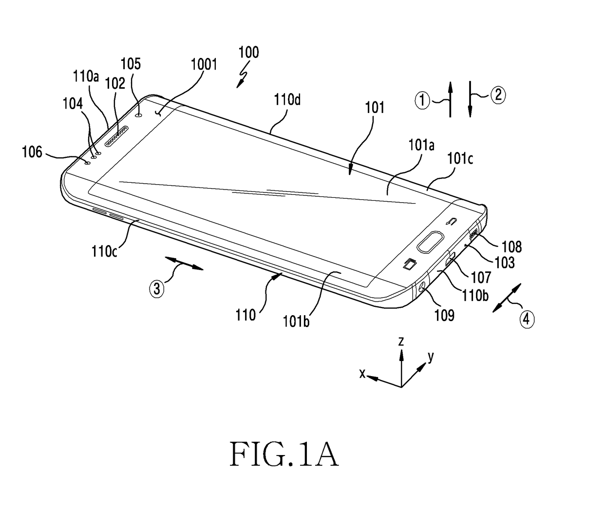
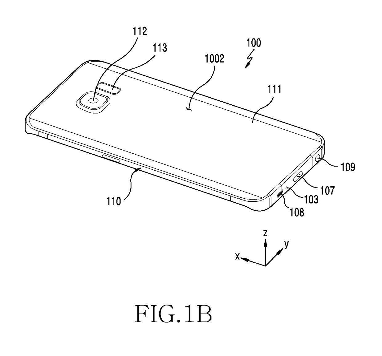
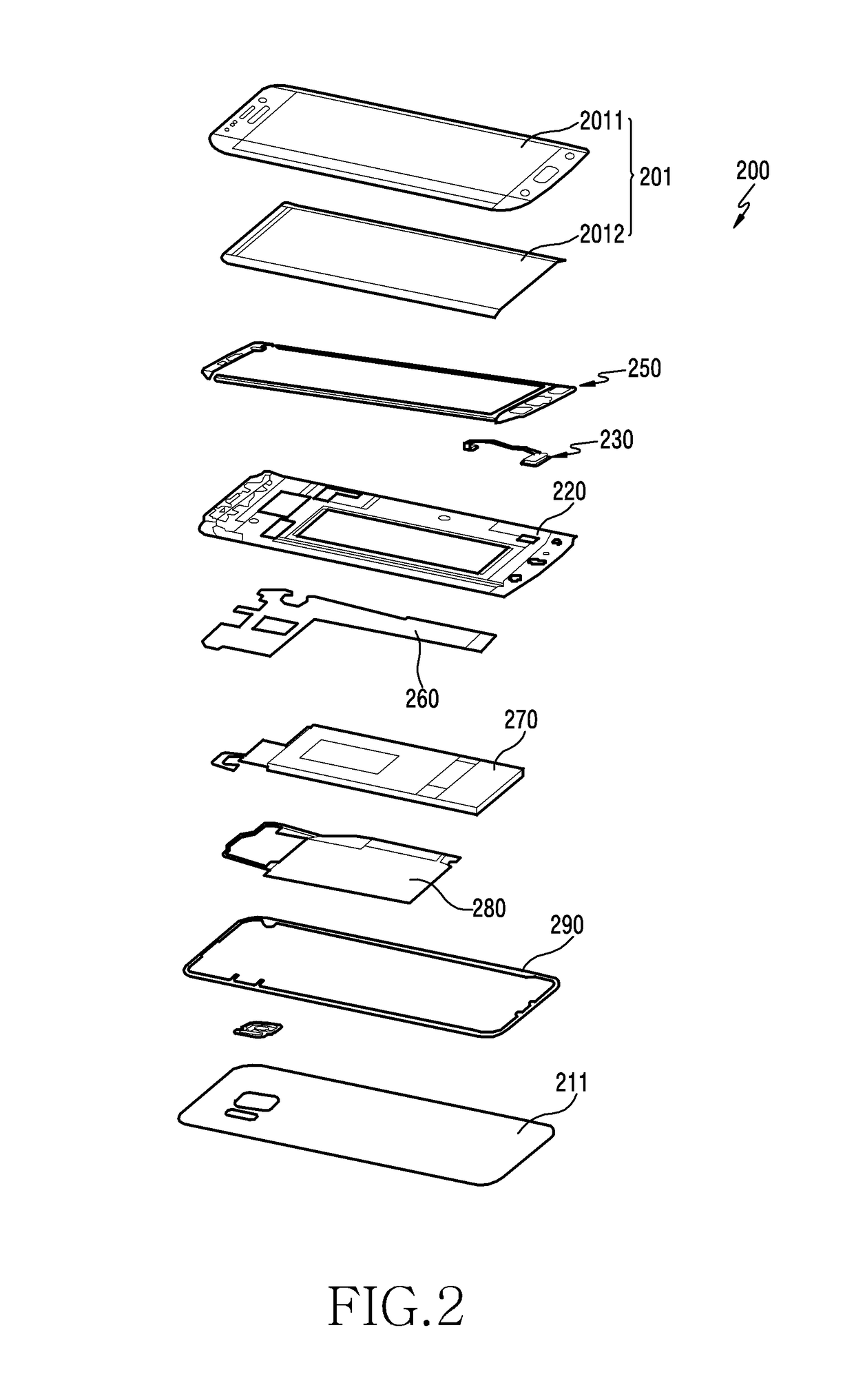
[0037]Hereinafter, various embodiments of the present disclosure are described with reference to accompanying drawings. However, the present disclosure is not limited to these specific embodiments, and it should be understood that modifications, equivalents, and / or alternatives of the embodiments described herein can be made.

[0038]With regard to description of drawings, similar components may be marked by similar reference numerals.

[0039]Terms and expression used in the present disclosure are used to describe specified embodiments of the present disclosure and are not intended to limit the scope of other embodiments. The terms of a singular form may include plural forms unless otherwise specified. Unless otherwise defined herein, all the terms used herein, which include technical or scientific terms, may have the same meaning that is generally understood by a person skilled in the art. Further, terms that are defined in a dictionary and commonly used, should also be interpreted as i...


PUM


Abstract

A circuit board is provided in which a transmission loss is reduced. The circuit board includes a first layer; a transmission line disposed on the first layer; and a second layer stacked with the first layer. The second layer includes a first region, which is constructed of a first material, corresponding to a position of the transmission line, and a second region, which is constructed of a second material having a permittivity that is different from that of the first material, corresponding to the position of the transmission line.

Description

CROSS REFERENCE TO RELATED APPLICATION(S)[0001]This application is based on and claims priority under 35 U.S.C. § 119 to Korean Patent Application No. 10-2017-0073976, filed on Jun. 13, 2017, in the Korean Intellectual Property Office, the disclosure of which is incorporated by reference herein in its entirety.BACKGROUND1. Field[0002]The present disclosure relates generally to a circuit board having a transmission line for reducing a transmission loss, and an electronic device including the circuit board.2. Description of Related Art[0003]When a high-frequency Radio Frequency (RF) signal is transmitted in a typical printed circuit board, a transmission loss occurs due to a physical property of the printed circuit board, thereby limiting a distance for transmitting the high-frequency RF signal. For example, the transmission loss may be caused by a conductor and / or a dielectric material of the printed circuit board.[0004]In such a conventional printed circuit board, there is a problem...

Claims


Application Information

Patent Timeline
Patent Type & Authority Applications(United States)
IPC IPC(8): H05K1/02H05K5/00H01P3/08H01Q1/22
CPCH05K1/024H05K5/0017H01P3/08H01Q1/22H05K2201/10098H01P3/003H01P3/081H01P3/085H01Q1/243H01Q9/0421H01Q21/28H05K1/025H05K2201/0187H05K1/0237H05K1/0298
Inventor PARK, CHAN-GIMIN, YIKYUCHO, HAN MINYUN, YEONSANGHAM, TAE-WOOK
Owner SAMSUNG ELECTRONICS CO LTD
Why Eureka
Try Eureka