cmos contact fluorescence detection analysis array sensor chip

A fluorescence detection and array sensing technology, which is applied in fluorescence/phosphorescence, material excitation analysis, radiation control devices, etc., can solve the problems of reducing the sensitivity and loss of fluorescence detection, and achieve the effect of reducing signal transmission loss

Active Publication Date: 2016-05-18
ZHEJIANG UNIV OF TECH
View PDF12 Cites 2 Cited by
  • Summary
  • Abstract
  • Description
  • Claims
  • Application Information

AI Technical Summary

Problems solved by technology

[0004] Aiming at the problem that fluorescence will generate loss between the fluorescence reaction pool and the fluorescence detector during the test of the current fluorescence detection device and reduce the sensitivity of fluorescence detection, the present invention proposes a CMOS contact type fluorescence detection analysis with high test sensitivity and low loss array sensor chip

Method used


Image

  • cmos contact fluorescence detection analysis array sensor chip
  • cmos contact fluorescence detection analysis array sensor chip

Examples


Embodiment 1

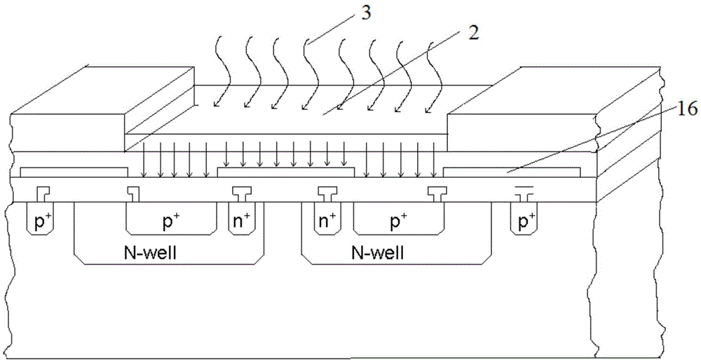
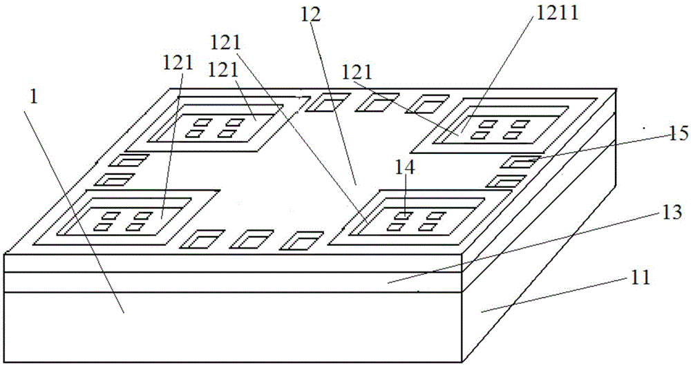
[0016] Embodiment 1 The CMOS contact-type fluorescent detection and analysis array sensor chip of the present invention includes a chip body 1, and the chip body includes a silicon substrate 11, SU-8 thick glue 12, a signal processing circuit 13, a photoelectric sensor Array 14, an active preprocessing amplification array and an asynchronous timing control circuit, the SU-8 thick glue 12 is fixed on the upper surface of the silicon substrate 11, and at least one fluorescent light is set on the SU-8 thick glue 12 Reaction cell group 121, each described fluorescent reaction cell group 121 is made of at least one micro-reaction cell 1211; The corresponding signal processing circuit 13, photoelectric sensor array are laid on the silicon substrate 11 that is positioned at the fluorescent reaction cell group 121 just below 14. Active preprocessing amplifying array and asynchronous timing control circuit; the signal input end of the photoelectric sensor array 14 is connected to the si...


PUM

PropertyMeasurementUnit
depthaaaaaaaaaa

Abstract

The invention relates to a CMOS (Complementary Metal-Oxide-Semiconductor Transistor) contact type fluorescent homogeneous assay array sensing chip which comprises a chip body, wherein the chip body comprises a silicon gel substrate, an SU-8 thick adhesive, a signal processing circuit, a photoelectric sensing array, an active preprocessing amplifying array and an asynchronous time sequence control circuit; the SU-8 thick adhesive is fixed on the upper surface of the silicon substrate, at least one florescent reaction pool group is arranged on the SU-8 thick adhesive, each florescent reaction pool group comprises at least one micro-reaction pool, and the signal processing circuit, the photoelectric sensing array, the active preprocessing amplifying array and the asynchronous time sequence control circuit are correspondingly laid on the silicon gel substrate positioned just below the florescent reaction pool group; the signal output end of the signal processing circuit is connected with a pressure welding block. The CMOS contact type fluorescent homogeneous assay array sensing chip has the beneficial effects that a photoelectric PN junction diode is capable of converting fluorescent into a photoelectric current; the photoelectric PN junction diode is integrated with the active signal processing circuit monolithically, thus the signal transmission loss is reduced, and the detection microminiaturization is realized; the micro-reaction pool is capable of detecting one sample or simultaneously detecting a plurality of samples.

Description

technical field [0001] The invention relates to a CMOS contact fluorescent detection and analysis array sensor chip. Background technique [0002] Fluorescence detection methods have been widely used in gene information detection, virus detection, DNA sequence testing, etc. It is currently one of the most important and convenient detection technologies in the field of biochemistry. Commonly used detectors for fluorescence detection include photomultiplier tubes (PMTs), avalanche diodes (APDs), and charge-coupled devices (CCDs). Outputting a corresponding voltage value, the detection and signal processing of discrete components have the characteristics of large size, high price, high working voltage and incompatibility with CMOS technology. In the CMOS process, photosensitive devices with diode, triode or grating structure can be realized, and signal processing circuits can also be monolithically integrated. The detection equipment composed of these devices has the advantage...

Claims


Application Information

Patent Timeline
Patent Type & Authority Patents(China)
IPC IPC(8): G01N21/64H01L27/144
Inventor 施朝霞曹全君李如春
Owner ZHEJIANG UNIV OF TECH
Why Eureka
Try Eureka