Cascaded electrical device bus structure systems and methods

Active Publication Date: 2018-12-27
GENERAL ELECTRIC CO
View PDF3 Cites 3 Cited by
  • Summary
  • Abstract
  • Description
  • Claims
  • Application Information

AI Technical Summary

Benefits of technology

The patent text describes a method for designing a bus structure for an electrical system. The bus structure includes multiple layers, including conductive and non-conductive layers. The first conductive layer is formed on one side of the bus structure, while the second conductive layer is formed on the opposite side. The first non-conductive layer separates the first conductive layer from the second conductive layer, and the second non-conductive layer separates the second conductive layer from the fourth conductive layer. The fourth conductive layer is formed to reduce voltage overshoot in the electrical system when the bus structure is deployed. The fifth conductive layer is formed to facilitate electrically coupling at least two electrical devices in series. This invention helps to improve the stability and reliability of the electrical system.

Problems solved by technology

However, in some instances, switching between connecting and disconnecting electrical power to an electrical connector may introduce stray impedance (e.g., capacitance and / or inductance), which affects operation of the electrical system and / or surrounding electrical devices.
In some instances, stray inductance may result in voltage overshoot occurring in the electrical system, which may affect lifespan and / or operational reliability of electrical devices in the electrical system.

Method used


Image

  • Cascaded electrical device bus structure systems and methods
  • Cascaded electrical device bus structure systems and methods
  • Cascaded electrical device bus structure systems and methods

Examples


Embodiment Construction

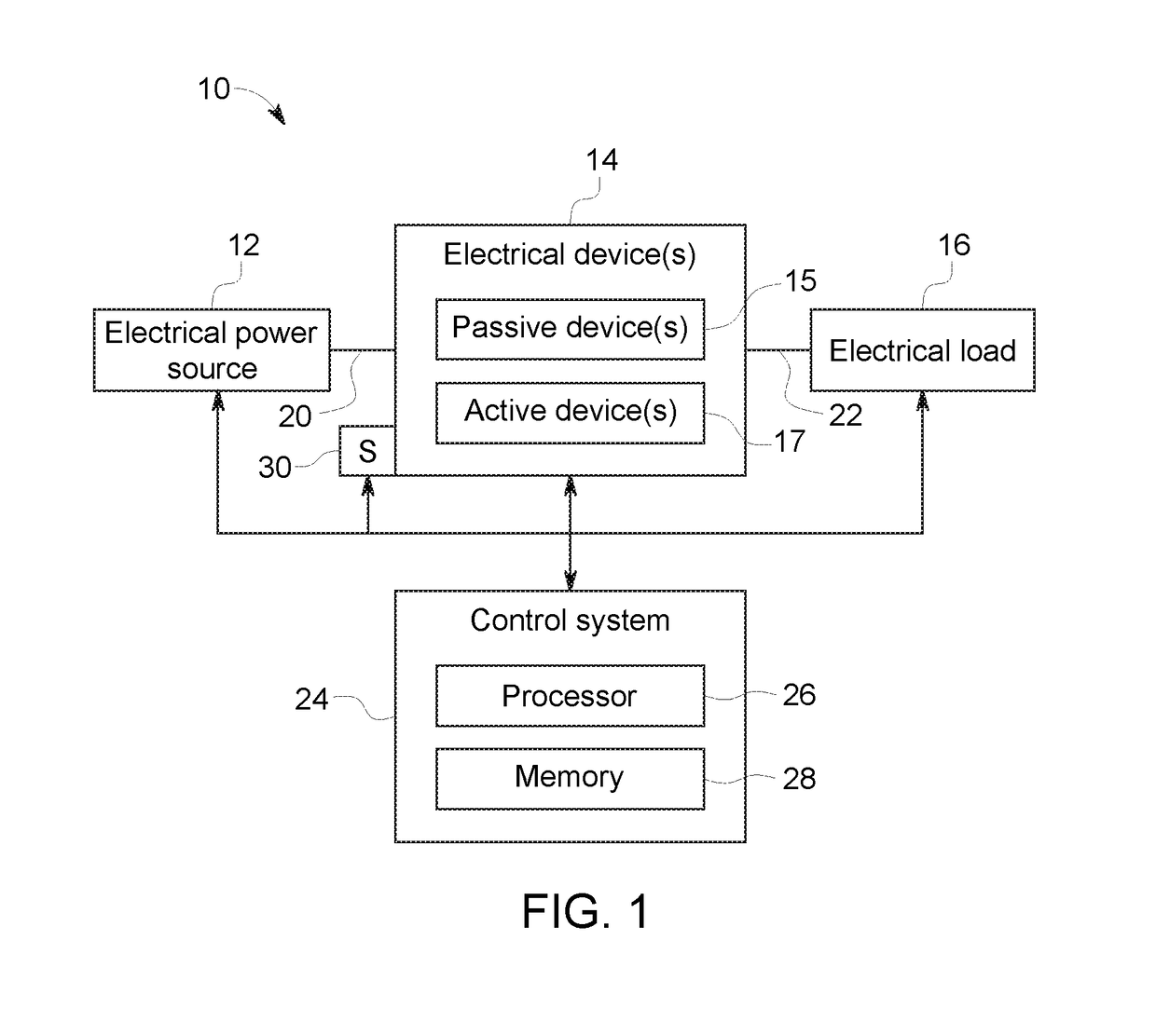
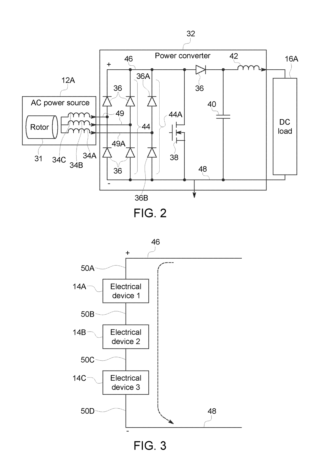
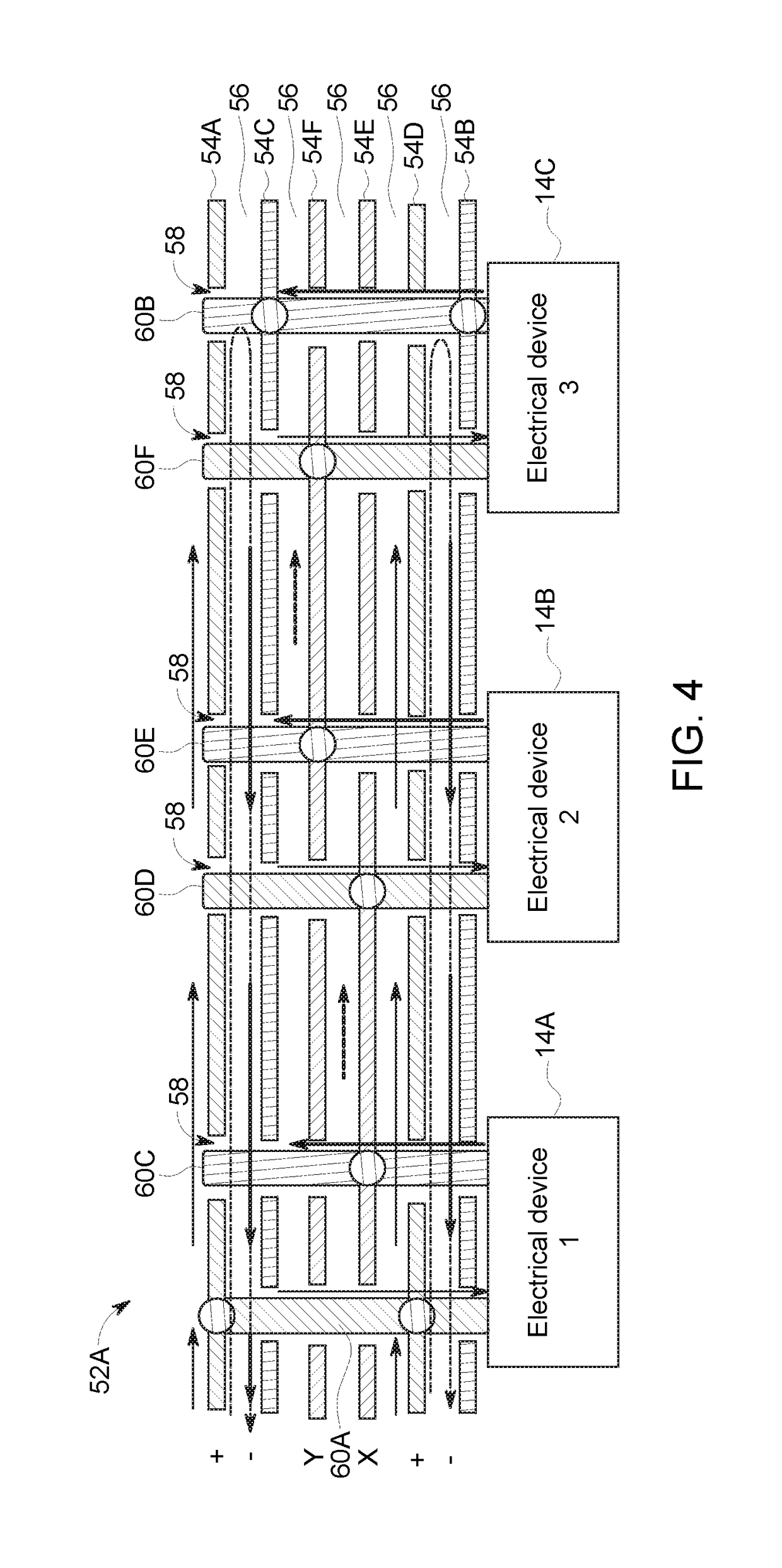
[0018]One or more specific embodiments of the present disclosure will be described below. These described embodiments are only examples of the presently disclosed techniques. Additionally, in an effort to provide a concise description of these embodiments, all features of an actual implementation may not be described in the specification. It should be appreciated that in the development of any such actual implementation, as in any engineering or design project, numerous implementation-specific decisions must be made to achieve the developers' specific goals, such as compliance with system-related and business-related constraints, which may vary from one implementation to another. Moreover, it should be appreciated that such a development effort might be complex and time consuming, but may nevertheless be a routine undertaking of design, fabrication, and manufacture for those of ordinary skill having the benefit of this disclosure.

[0019]When introducing elements of various embodiment...


PUM


Abstract

The present disclosure presents techniques to facilitate improving operation of an electrical system, which includes a bus structure that cascades multiple electrical devices. The bus structure includes a first outer conductive layer implemented as a positive layer; a second outer conductive layer implemented as a negative layer; a first intermediate conductive layer neighboring the first outer conductive layer; a second intermediate conductive layer neighboring the second outer conductive layer; and a third intermediate conductive layer neighboring the second intermediate conductive layer, in which the third intermediate conductive layer is implemented as an inter-device layer that facilitates electrically coupling at least two of the electrical devices in series. The first intermediate conductive layer is implemented as a negative layer and the second intermediate conductive layer is implemented as a positive layer to facilitate reducing stray inductance and / or increasing stray capacitance introduced in the electrical system during operation.

Description

BACKGROUND[0001]This section is intended to introduce the reader to various aspects of art that may be related to various aspects of the present techniques, which are described and / or claimed below. This discussion is believed to be helpful in providing the reader with background information to facilitate a better understanding of the various aspects of the present disclosure. Accordingly, it should be understood that these statements are to be read in this light, and not as admissions of prior art.[0002]Generally, an electrical system may include multiple electrical devices electrically interconnected to facilitate supplying electrical power from an electrical power source (e.g., generator) to an electrical load. In some instances, the electrical devices may include a passive electrical device, such as a capacitor or an inductor, and / or an active electrical device that may be operationally controlled, such as an electromechanical switching device or a semiconductor switching device...

Claims


Application Information

Patent Timeline
IPC IPC(8): G02B26/00H02G5/00G01R33/04G01R35/04G01R22/00
CPCG02B26/001H02G5/007G01R22/00G01R35/04G01R33/04H01B5/14H01R4/58H02M7/12H02M7/003G01R33/093
Inventor WANG, RUXILINK, DOUGLASFREEMAN, MELISSATAO, FENGFENGSABATE, JUAN ANTONIODELGADO, ELADIO CLEMENTE
Owner GENERAL ELECTRIC CO
Why Eureka
Try Eureka