Method of manufacturing chemical fluid for manufacturing electronic material, pattern forming method, method of manufacturing semiconductor device, chemical fluid for manufacturing electronic material, container, and quality inspection method

a chemical fluid and electronic material technology, applied in the field of methods, can solve problems such as performance degradation, and achieve the effect of efficient manufacturing

Active Publication Date: 2019-01-10
FUJIFILM CORP
View PDF2 Cites 6 Cited by
  • Summary
  • Abstract
  • Description
  • Claims
  • Application Information

AI Technical Summary

Benefits of technology

[0042]According to the present invention, it is possible to provide a method of manufacturing a chemical fluid for manufacturing an electronic material that can highly efficiently manufacture a high-quality chemical fluid for manufacturing an electronic material even in the forming of an ultrafine pattern (for example, having a node of 10 nm or lower), a pattern forming method and a method of manufacturing a semiconductor device using the same, a high-quality chemical fluid for manufacturing an electronic material even in the forming of the ultrafine pattern and a container, and a quality inspection method particularly in the forming of the ultrafine pattern.

Problems solved by technology

It is known that contamination of unintentional metal impurities into a chemical fluid for manufacturing an electronic material used for manufacturing a semiconductor device causes performance deterioration of a semiconductor device, and thus in the chemical fluid for manufacturing the electronic material having a node of up to about 20 nm, control of a metal impurity concentration of about several tens of ppb is required.

Method used


Image

  • Method of manufacturing chemical fluid for manufacturing electronic material, pattern forming method, method of manufacturing semiconductor device, chemical fluid for manufacturing electronic material, container, and quality inspection method
  • Method of manufacturing chemical fluid for manufacturing electronic material, pattern forming method, method of manufacturing semiconductor device, chemical fluid for manufacturing electronic material, container, and quality inspection method
  • Method of manufacturing chemical fluid for manufacturing electronic material, pattern forming method, method of manufacturing semiconductor device, chemical fluid for manufacturing electronic material, container, and quality inspection method

Examples


example 1

[0148]After 5 L of the washing solution charges a container with an inner volume of 20 L, the container is tightly sealed. Shaking stirring is performed for one minute such that the washing solution is spread over the entire surface of a liquid contact portion in the container evenly, and then the lid is opened to discharge the washing solution. Substitution is performed three times with ultrapure water so as to be sufficiently rinsed and ultrapure water is dried. The number of times and the time of washing with the washing solution and, if necessary, the number of times and the time of rinsing with ultrapure water afterwards may be determined depending on the required cleanliness.

example 2

[0149]The opening of the container is downward faced, and the washing solution is jetted from the opening through the jetting nozzle or the like to the inner surface of the container for washing. Washing or the like is appropriately performed such that the entire inner surface of the container is washed by using a diffusion nozzle, providing a plurality of nozzles, and operating the container and / or a washing nozzle. Washing time is determined depending on the required cleanliness.

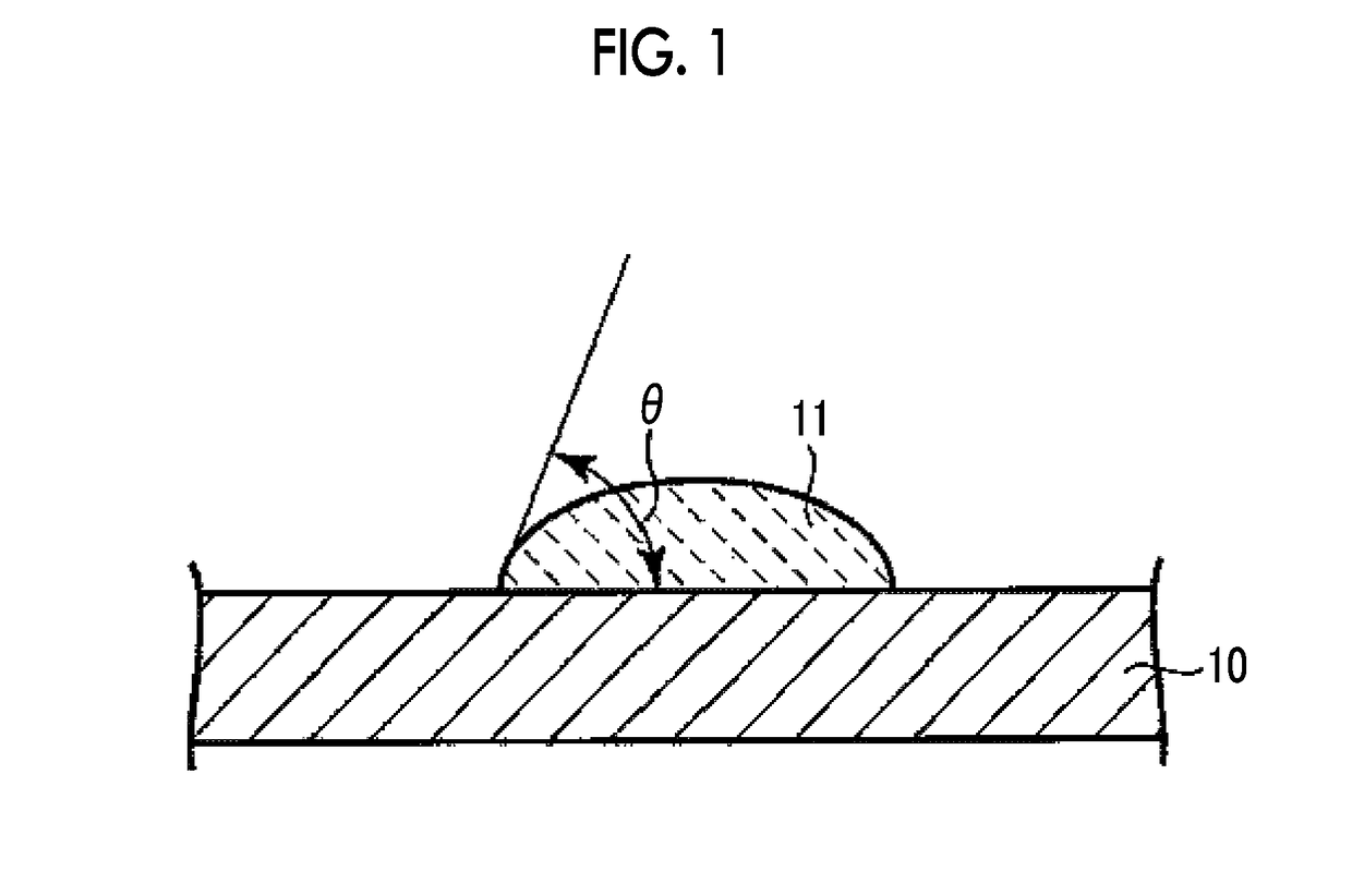
[0150]According to an aspect, the container of the present invention is a container holding the chemical fluid for manufacturing an electronic material, and in this container, a proportion (hereinafter, referred to as a “void volume”) of a void occupying the holding portion that holds the chemical fluid for manufacturing an electronic material is preferably 50 to 0.01 vol %. By causing an upper limit value of the void volume in the holding portion to be 50 vol % or less, it is possible to reduce the possib...

examples

[0623]Hereinafter, the present invention will be described in more detail with reference to examples, but the present invention is not limited thereto.


PUM

PropertyMeasurementUnit
median diameteraaaaaaaaaa
pore sizeaaaaaaaaaa
pore sizeaaaaaaaaaa

Abstract

In a method of manufacturing a chemical fluid for manufacturing an electronic material, a method of reducing particulate metal in the chemical fluid is selected according to a concentration of particulate metal including an iron atom, a concentration of particulate metal including a copper atom, and a concentration of particulate metal including a zinc atom which are measured by SP ICP-MS in the chemical fluid, and at least one of the concentration of particulate metal including an iron atom, the concentration of particulate metal including a copper atom, or the concentration of particulate metal including a zinc atom is reduced by using the selected reducing method.

Description

CROSS-REFERENCE TO RELATED APPLICATIONS[0001]This application is a Continuation of PCT International Application No. PCT / JP2017 / 12440, filed on Mar. 27, 2017, which claims priority under 35 U.S.C. § 119(a) to Japanese Patent Application No. 2016-072917, filed on Mar. 31, 2016 and Japanese Patent Application No. 2017-044273, filed on Mar. 8, 2017. Each of the above application(s) is hereby expressly incorporated by reference, in its entirety, into the present application.BACKGROUND OF THE INVENTION1. Field of the Invention[0002]The present invention relates to a method of manufacturing a chemical fluid for manufacturing an electronic material, a pattern forming method, a method of manufacturing a semiconductor device, a chemical fluid for manufacturing an electronic material, a container, and a quality inspection method.2. Description of the Related Art[0003]In the related art, various configurations are suggested as a positive tone pattern forming method using an alkali developer an...

Claims


Application Information

Patent Timeline
Patent Type & Authority Applications(United States)
IPC IPC(8): G03F1/00G03F1/86G03F7/32G03F7/38H01J49/10
CPCG03F1/0092G03F1/86H01J49/105G03F7/38G03F7/325G03F7/11G03F7/32G03F7/40G03F7/0012G03F7/0397G03F7/16G03F7/26G03F7/42H01L21/027G03F1/68
Inventor SHIMIZU, TETSUYAYAMANAKA, TSUKASAKAWADA, YUKIHISA
Owner FUJIFILM CORP
Why Eureka
Try Eureka