Image sensor and a method of operating the same

a technology of image sensor and image, applied in the field of image sensor, can solve the problems of flickering led, unwanted motion artifacts, etc., and achieve the effects of high contrast, high dynamic range, and reduced implementation cos

Active Publication Date: 2019-01-10
HIMAX IMAGING LIMITED
View PDF0 Cites 11 Cited by
  • Summary
  • Abstract
  • Description
  • Claims
  • Application Information

AI Technical Summary

Benefits of technology

[0006]In view of the foregoing, it is an object of the embodiment of the present invention to provide a method of operating an image sensor with high dynamic range without motion artifacts. The embodiment is capable of capturing high contrast scenes without saturation. The embodiment is capable of reducing cost of implementing, for example, 120 dB dynamic range by reading out at least three exposure values using two photodiodes in a pixel. The embodiment is also capable of mitigating LED flickering.

Problems solved by technology

Nevertheless, unwanted motion artifacts are present as the integration time of the long exposure and short exposure do not overlap.
When integration time of a particularly photodiode in a pixel is shorter than the ON duty cycle of the LED, the pixel will sometimes miss the LED signal, resulting in flickering of the LED.

Method used


Image

  • Image sensor and a method of operating the same
  • Image sensor and a method of operating the same
  • Image sensor and a method of operating the same

Examples


first embodiment

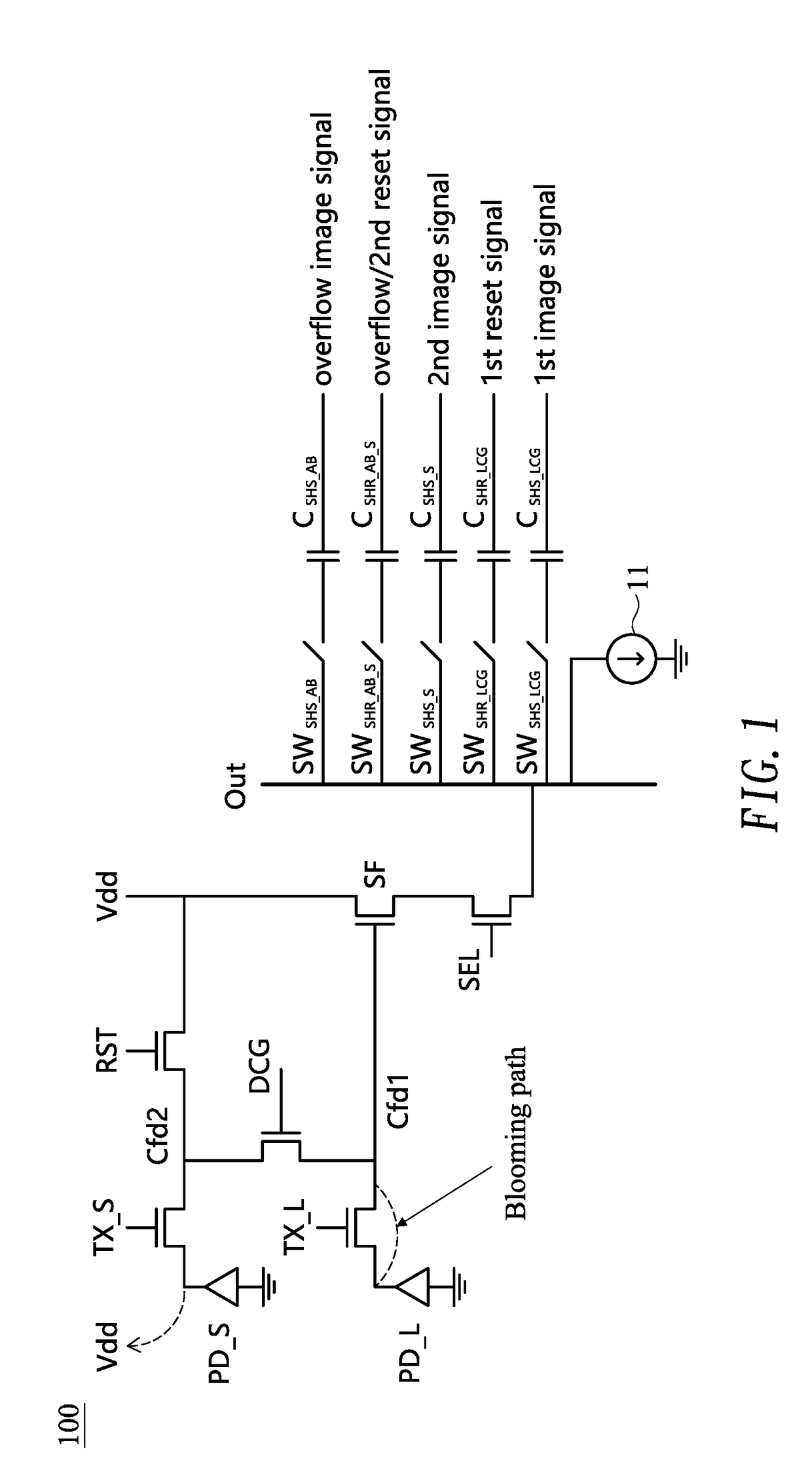
[0017]FIG. 1 shows a circuit diagram illustrated of a pixel circuit 100 of an image sensor (e.g., a complementary metal-oxide-semiconductor (CMOS) image sensor) according to the present invention. The pixel circuit 100 of the embodiment adopts four-transistor (4T) pixel architecture.

[0018]In the embodiment, the pixel circuit 100 may include a large (or first) photodiode PD_L and a small (or second) photodiode PD_S. The large photodiode PD_L has a photodiode area larger than the small photodiode PD_S. The anodes of the large photodiode PD_L and the small photodiode PD_S are connected to ground. Details of splitting a photodiode into a large photodiode and a small photodiode may be referred to “A 1280×1080 4.2 μm Split-diode Pixel HDR Sensor in 110 nm BSI CMOS Process,” entitled to Trygve Willassen et al., the disclosure of which is incorporated herein by reference.

[0019]The pixel circuit 100 may include a first transfer transistor TX_L connected between (a cathode of) the large photo...

second embodiment

[0035]FIG. 5 shows a circuit diagram illustrated of a pixel circuit 500 of an image sensor (e.g., a CMOS image sensor) according to the present invention. The pixel circuit 500 of the embodiment is similar to the pixel circuit 100 (FIG. 1) with the exception that the switches (e.g., SWSHS_AB, SWSHR_AB_S, SWSHS_S, SWSHR_LCG, SWSHS_LCG, SWSHR_HCG and SWSHS_HCG) connected to the output node and the capacitors (e.g., CSHS_AB, CSHR_AB_S, CSHS_S, CSHR_LCG, CSHS_LCG, CSHR_HCG and CSHS_HCG) associatively and respectively connected with the switches in series are to an extent different from the pixel circuit 100. Details of the switches and the associated capacitors of the embodiment will be described in details later in the specification.

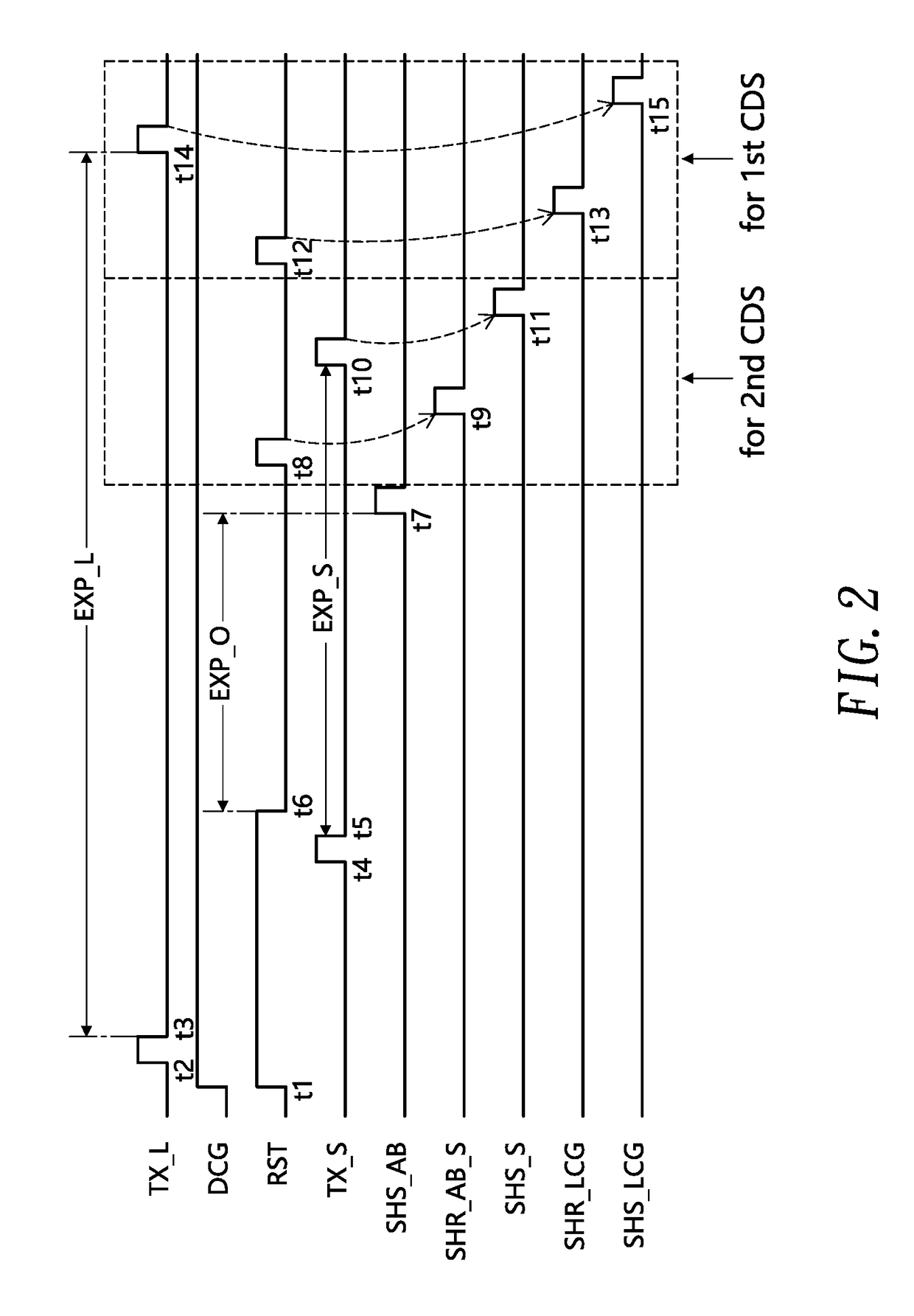
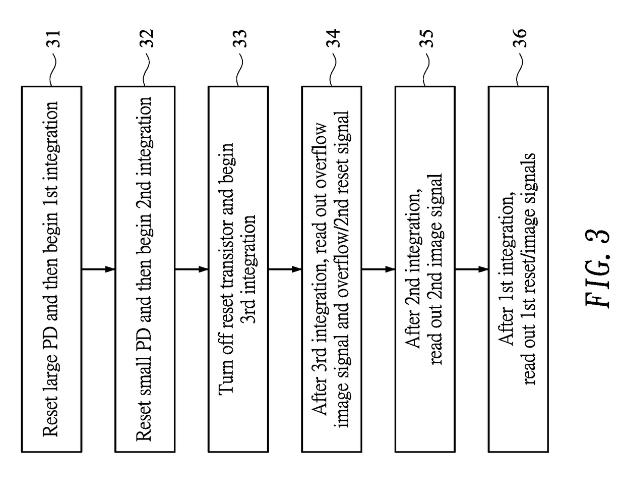
[0036]FIG. 6 shows an exemplary timing diagram illustrated of pertinent signals of the pixel circuit 550 of FIG. 5. The flow diagram of FIG. 3 illustrated of a method of operating an image sensor may be adapted to the pixel circuit 500 of FIG. 5. In the sec...


PUM


Abstract

The invention is directed to a method of operating an image sensor. A first integration is performed on a first photodiode of a pixel circuit to obtain at least one first image signal. A second integration is performed on a second photodiode of the pixel circuit to obtain a second image signal, the first photodiode having a photodiode area larger than the second photodiode. A third integration is performed by collecting blooming charge overflowing from the first photodiode to obtain an overflow image signal. The first integration has longest integration time and the third integration has shortest integration time among the first integration, the second integration and the third integration.

Description

BACKGROUND OF THE INVENTION1. Field of the Invention[0001]The present invention generally relates to an image sensor, and more particularly to a method of operating an image sensor with high dynamic range.2. Description of Related Art[0002]A complementary metal-oxide-semiconductor (CMOS) image sensor has been widely applied to mobile applications. The CMOS image sensor may be applied to other applications such as automotive and security applications. Requirements for the automotive and security applications are quite different from that for the mobile applications. For example, one strong request is high dynamic range (HDR), with which ultra dim and bright scenes can be captured at the same frame and with good quality.[0003]Dynamic range of pixel can be extended by splitting a single pixel into two photodiodes, one small and one large. Nevertheless, unwanted motion artifacts are present as the integration time of the long exposure and short exposure do not overlap.[0004]Light-emitti...

Claims


Application Information

Patent Timeline
Patent Type & Authority Applications(United States)
IPC IPC(8): H04N5/359H04N5/374H04N5/363H04N5/378
CPCH04N5/359H04N5/374H04N5/363H04N5/378H04N25/585H04N25/583H04N25/621H04N25/778H04N25/75H04N25/533H04N25/616
Inventor CHEUNG, YU HIN DESMONDMITTRA, AMITWU, YANG
Owner HIMAX IMAGING LIMITED
Why Eureka
Try Eureka