An optical apparatus

a technology of optical apparatus and optical modulator, applied in the field of optical modulators, can solve the problems of inherently lossless process of guiding optical signals (light) through dielectric structures, almost non-existent thermal noise, and mainly observed loss in practice, so as to achieve extremely energy-efficient high-speed optical modulators, enhance energy efficiency, and reduce the capacitance of each individual element.

Active Publication Date: 2019-01-17
PHOELEX
View PDF0 Cites 3 Cited by
  • Summary
  • Abstract
  • Description
  • Claims
  • Application Information

AI Technical Summary

Benefits of technology

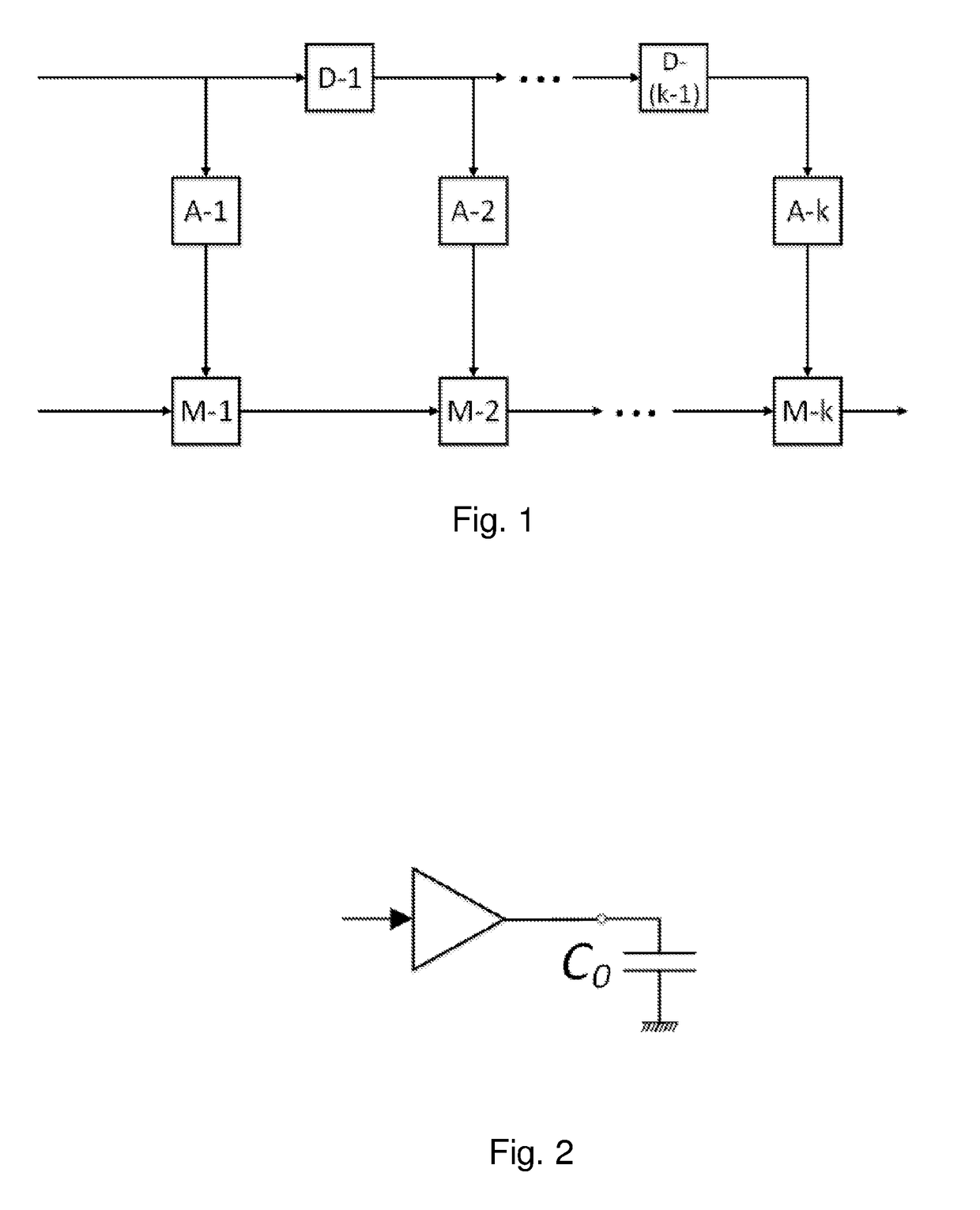
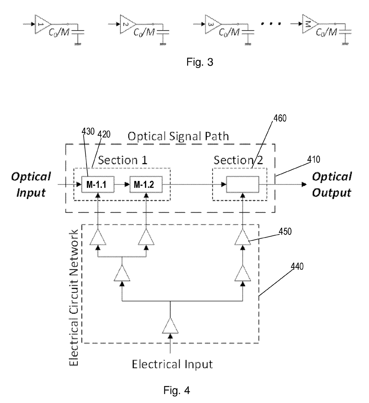
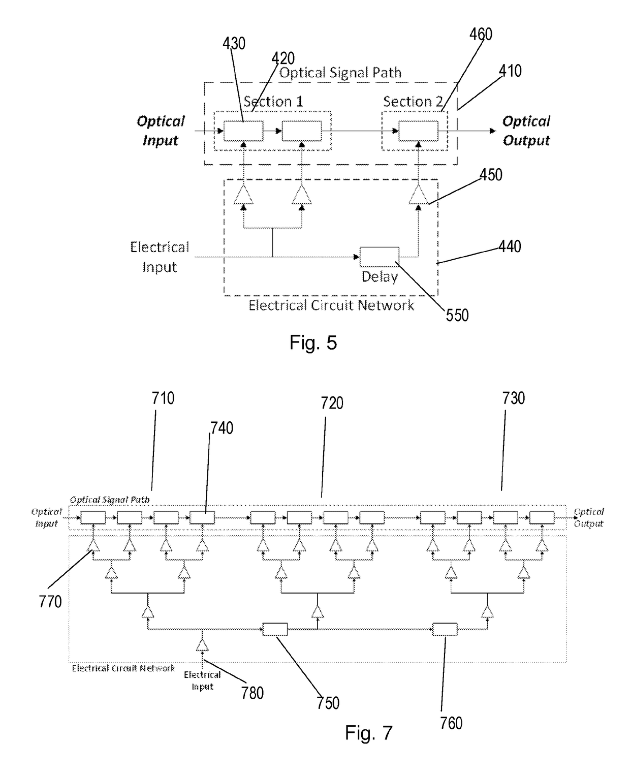
[0027]This invention discloses a general structure for extremely energy efficient high speed optical modulators. In the present invention, the original electrode is divided into sections and subsections, in order to reduce the capacitance of each individual element to as low as possible, resulting in dramatic enhancement of energy efficiency. Delays are provided between “sections” to emulate the operation of a traveling wave modulator, i.e., matching the timing of electrical and optical signals, henceforth increasing the speed (bandwidth) of the apparatus. Between “sub-sections” of a section, however, the time delays (phase changes) among the electrical signals driving the modulating elements are substantially minimised, henceforth, the overall energy efficiency of the apparatus is improved.

Problems solved by technology

First, the carrier frequency of optical signals, at hundreds of THz, is far away from the peak of black body radiation curve, and as such thermal noise is almost nonexistent.
Second, unlike the process of guiding electrical signals through metallic structures which is inherently lossy, the process of guiding optical signals (light) through dielectric structures is inherently lossless, and the loss observed in practice is mostly the result of manufacturing imperfections rather than any fundamental physical phenomena.
However, in the case of semiconductor modulators, for instance silicon modulators, the situation is dramatically different.
Consequently, the engineering effort for design and optimization often requires making delicate tradeoffs among competing performance metrics.
On the flip side, larger doping concentrations detrimentally affect the attenuation of RF signals driving the electrical ports, acting as a limiting factor in the speed of operation.
However, the biggest disadvantage of the technique is that, it is not energy efficient.
This prior art does not have the intention of obtaining energy efficiency or power efficiency.
Therefore, if more modulator elements are used, more delay elements are necessary, which increases both complexity and energy consumption.
Adjusting the output amplitude of most drivers to accomplish this goal is problematic; it usually results in a change in edge rate (i.e., transition time between an optical “1” and optical “0”) and, depending on driver topology, might not reduce power dissipation.
Therefore, it has been found that the extinction ratio of the output optical signal can be adjusted (While maintaining a constant electrical swing on the drive voltage) by dynamically adjusting the effective length of the modulated portion of the modulator structure.” Again here, the requirement that all drivers have to energize / de-energize “separately” is the biggest limitation of this prior art, and we will remove this limitation as explained later to significantly reduce energy dissipation.
This is a major limitation of this prior art.
However, traveling-wave electrodes exhibiting sharp bends needed for such folded paper-clip structures experience large losses at high frequencies, in addition to all the disadvantages that have been described before.
This prior art again, by virtue of previous explanations, requires high voltage drivers and as such silicon based drivers cannot be used.

Method used


Image

  • An optical apparatus
  • An optical apparatus
  • An optical apparatus

Examples


Embodiment Construction

[0196]The invention will be described in respect of general theory of the invention first and then will be described in respect of various preferred embodiments.

[0197]The group velocity limited bandwidth (BW) of a traveling wave optical modulator is given by the following approximate relation [1],

BW≃1.4cπLng-nRF

in which BW is the modulator bandwidth in hertz (Hz), c is the vacuum speed of light, L is the interaction length of the modulator (the length along which optical and RF fields travel together), ng is the group index of the optical field and nRF is the group index of the RF field, which are related to the propagation velocities of the optical (vg) and RF (vRF) fields, through following relations,

vg=c / ng

and

vRF=c / nRF.

[0198]As it is evident, in order to obtain wideband operation (large values of BW), one should either decrease the length L or bring the values of ng and nRF close to each other.

[0199]To get better understanding, two examples are considered below.

[0200]Modulators ...


PUM

PropertyMeasurementUnit
time delayaaaaaaaaaa
time-of-flightaaaaaaaaaa
electricalaaaaaaaaaa

Abstract

We disclose herein an optical apparatus comprising an optical signal path which is driven by a plurality of electrical drivers. The electrical drivers are configured to optimise delays between two adjacent electrical drivers. The delays are optimised such that power loss in the optical apparatus is reduced.

Description

FIELD OF INVENTION[0001]The present invention relates generally to optical apparatuses, particularly but not exclusively, to optical modulators.BACKGROUND OF INVENTION[0002]The backbone infrastructure on which “information technology” is running, comprises two major parts, “information processing” and “information transfer”. The information processing is done in electrical domain by exploiting ubiquitous transistors (subject of Shockley-Bardeen-Brattain's 1956 physics Nobel prize) which are integrated in quantities of millions to tens of billions in tiny integrated circuits (subject of Jack Kilby's 2000 physics Nobel prize). The frequencies at which these circuits are operating are normally in the range of tens of hertz (Hz) to tens of giga-hertz (GHz).[0003]However, when it comes to the transfer of information, electrical signals exhibit major shortcomings, whereas signals at optical frequencies, i.e., frequencies in the range of hundreds of tera-hertz (THz), have significant advan...

Claims


Application Information

Patent Timeline
Patent Type & Authority Applications(United States)
IPC IPC(8): G02F1/01G02F1/225G02F1/025
CPCG02F1/0121G02F1/225G02F2001/211G02F2001/212G02F1/025G02F1/01G02F1/011G02F1/2255G02F1/211G02F1/212G02F1/21G02B6/10G02B2006/12142G02F1/0151G02F1/0154H04B10/5053H04B10/541
Inventor NEJADMALAYERI, AMIR HOSSEIN
Owner PHOELEX
Why Eureka
Try Eureka