Integrated electronic device with a redistribution region and a high resilience to mechanical stresses

a technology of integrated electronic devices and mechanical stresses, applied in the direction of solid-state devices, electric devices, basic electric elements, etc., can solve problems such as stress, and achieve the effect of high thermal budg

Inactive Publication Date: 2019-01-31
STMICROELECTRONICS SRL
View PDF6 Cites 11 Cited by
  • Summary
  • Abstract
  • Description
  • Claims
  • Application Information

AI Technical Summary

Benefits of technology

[0027]In light of the above, because of the different mechanical characteristics of the materials that form the redistribution layer 25, the first dielectric layer 11 and the first and second coating layers 30, 32, it is possible for the integrated electronic device 10 to be subjected to excessive mechanical stresses, which may compromise its operation. In particular, the stresses arise for example in the case in which the fabrication process includes the execution of steps with a high thermal budget.

Problems solved by technology

In particular, the stresses arise for example in the case in which the fabrication process includes the execution of steps with a high thermal budget.

Method used


Image

  • Integrated electronic device with a redistribution region and a high resilience to mechanical stresses
  • Integrated electronic device with a redistribution region and a high resilience to mechanical stresses
  • Integrated electronic device with a redistribution region and a high resilience to mechanical stresses

Examples


first embodiment

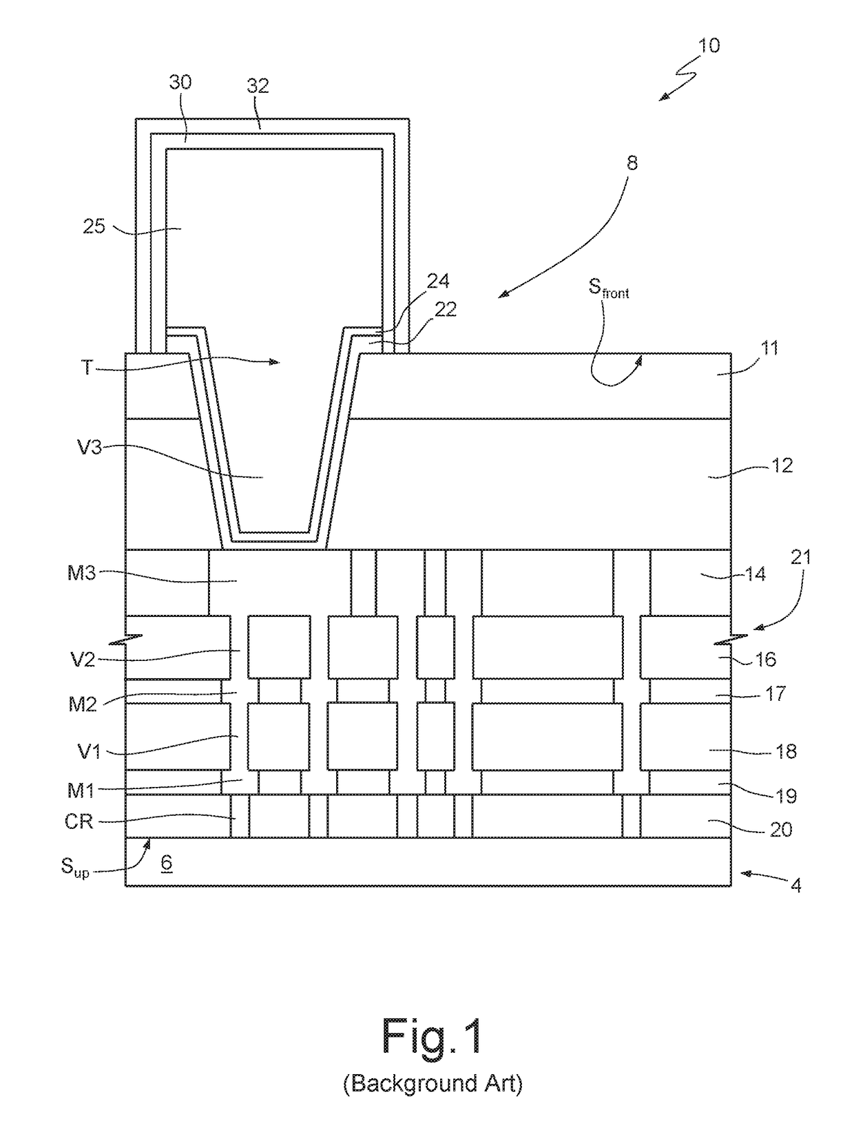
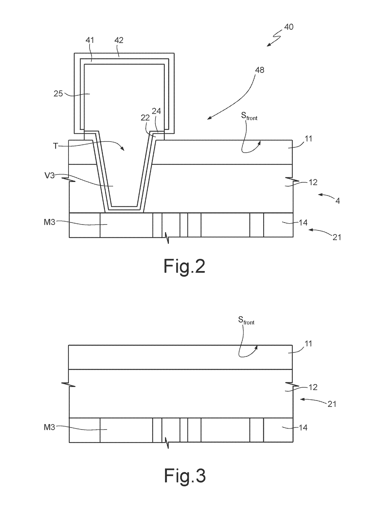
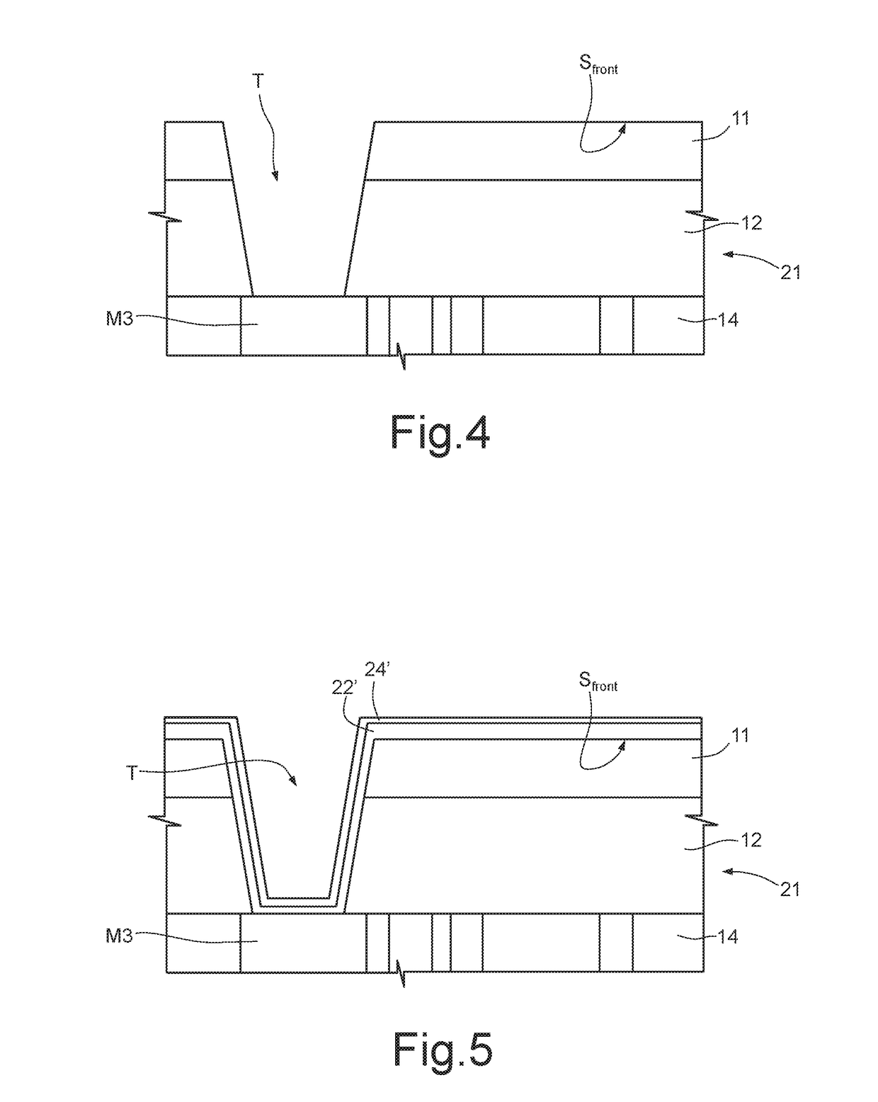
[0037]the present integrated electronic device is shown in FIG. 2, where it is indicated with 40. In particular, FIG. 2 shows only an upper portion of the integrated electronic device 40, given that the elements disposed underneath the third dielectric layer 14 are not shown.

[0038]This having been said, the first coating layer, here indicated with 41, covers the top and the sides of an upper portion of the redistribution layer 25 and is disposed at a distance from the first dielectric layer 11, i.e., it is physically separated from the latter. Furthermore, the first coating layer 41 is physically separated from the first patterned barrier layer 22 and from the patterned seed layer 24, given that it extends at the bottom to a height which is higher than the maximum height reached by the patterned seed layer 24. Consequently, the first coating layer 41 leaves a lower portion of the redistribution layer 25 laterally exposed, together with portions of the patterned seed layer 24 and of ...


PUM

PropertyMeasurementUnit
thicknessesaaaaaaaaaa
thicknessaaaaaaaaaa
thicknessaaaaaaaaaa

Abstract

An integrated device includes a semiconductor body and a dielectric layer bounded by a surface. A conductive region of a first metal material forms a via region extending into a hole passing through the dielectric layer, and an overlaid redistribution region which extends over the surface. At least one barrier region of a second metal material extends into the hole and surrounds the via region, and the barrier region furthermore extending over the surface. A first coating layer of a third metal material covers the top and the sides of an upper portion of the redistribution region at a distance from the surface. A second coating layer of a fourth metal material extends at a distance from the surface and covers the first coating layer, and covers laterally a lower portion of the redistribution region which is disposed on top of portions of the barrier region extending over the surface.

Description

BACKGROUNDTechnical Field[0001]The present disclosure relates to an integrated electronic device, which includes a redistribution region and has a high resilience to mechanical stresses.Description of the Related Art[0002]As is known, in the field of technologies for fabricating semiconductor circuits, reference is generally made to the redistribution layer (RDL) in order to indicate an additional metal layer of an integrated circuit (“chip”) formed within a die, which allows the input / output pads (I / O) formed within the same die to be rendered electrically accessible. In other words, the redistribution layer is a metal layer connected to the I / O pads, to which the wires which allow the ‘wire bonding’ may, for example, be connected in different positions with respect to the positions in which the pads are disposed. The redistribution layer thus allows, for example, the processes of electrical connection between chips to be simplified.[0003]One example of use of the redistribution la...

Claims


Application Information

Patent Timeline
Patent Type & Authority Applications(United States)
IPC IPC(8): H01L23/522H01L21/768H01L23/532
CPCH01L2224/04042H01L23/53238H01L2224/03462H01L2224/05009H01L21/76846H01L21/76852H01L21/76873H01L21/7688H01L2224/05017H01L2224/0508H01L2224/05181H01L2224/05166H01L2224/05027H01L2224/05187H01L2224/05083H01L2224/05084H01L2224/05147H01L2224/05558H01L2224/05644H01L2224/05564H01L2224/05583H01L2224/05563H01L2224/4809H01L2224/05582H01L2224/05655H01L2224/48175H01L2924/04941H01L24/03H01L24/05H01L24/48H01L23/5226H01L21/76802H01L2224/03005H01L21/76885H01L23/5283H01L24/02H01L2221/1078H01L2224/0233H01L2224/02331H01L2224/0239H01L2224/03001H01L2224/03464H01L2224/0347H01L2224/03614H01L2224/0381H01L2224/03825H01L2224/039H01L2224/03901H01L2224/03914H01L2224/05008H01L2224/05548H01L2224/05566H01L2224/48091H01L2224/48247H01L2924/00014H01L2924/351H01L2924/00012H01L2924/01029H01L2924/01015H01L2924/01074H01L2924/01042H01L2924/01028H01L2224/034H01L2924/01022H01L2924/01073H01L2924/04953H01L2924/01046H01L2924/01079H01L2224/45099
Inventor VENEGONI, IVANMILANESI, FRANCESCAPIPIA, FRANCESCO MARIASCIARRILLO, SAMUELECOLPANI, PAOLO
Owner STMICROELECTRONICS SRL
Why Eureka
Try Eureka