
Light emitting element and method for fabricating the same

a technology solder, which is applied in the direction of basic electric elements, electrical equipment, semiconductor devices, etc., can solve the problems of reducing affecting the luminous efficiency of light emitting elements, and affecting the reliability of electrical conductivity and solder, so as to reduce the amount of solder used, and improve the effect of ligh

Active Publication Date: 2019-02-21
LUMENS
View PDF2 Cites 7 Cited by
  • Summary
  • Abstract
  • Description
  • Claims
  • Application Information

AI Technical Summary

Benefits of technology

The present invention provides a light emitting element with improved luminous efficiency and a method for fabricating it using an IR laser to bond an LED chip to a substrate through a solder. The invention prevents squeazed-out solder from lowering the luminous efficiency of the light emitting element. The use of IR laser minimizes the generation of flux and ensures uniform heating of the solder, leading to high electrical conductivity and reliability of the solder. The invention also ensures stable and reliable bonding through maximizing the areas of the solder portions in contact with the inner portions of the electrodes.

Problems solved by technology

However, the solder covers the lateral sides of the LED chip and absorbs light emitted from the LED chip, with the result that the about 3% to about 4% of the light is lost.
Further, flux remaining in the light emitting element tends to discolor, resulting in an unwanted change in color coordinates.
Moreover, non-uniform heat applied to the solder during reflow soldering causes a difference in the degree of melting, resulting in the formation of voids that deteriorate the electrical conductivity and reliability of the solder.
The inspection of bonding defects is also inaccurate.

Method used


Image

  • Light emitting element and method for fabricating the same
  • Light emitting element and method for fabricating the same
  • Light emitting element and method for fabricating the same

Examples


Embodiment Construction

[0026]Preferred embodiments of the present invention will now be described with reference to the accompanying drawings. It should be noted that the drawings and embodiments are simplified and illustrated such that those skilled in the art can readily understand the present invention, and therefore, they should not be construed as limiting the scope of the present invention.

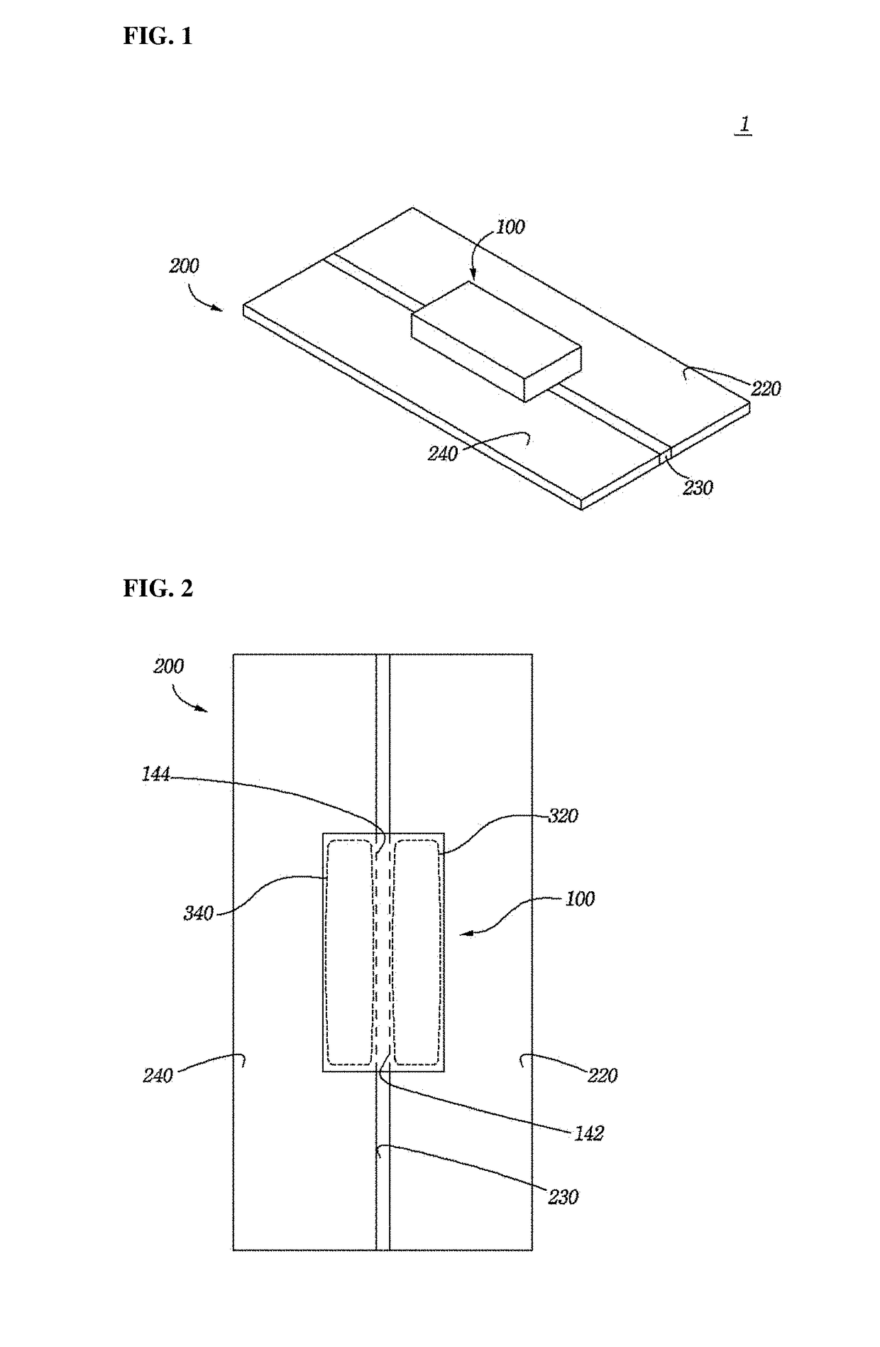
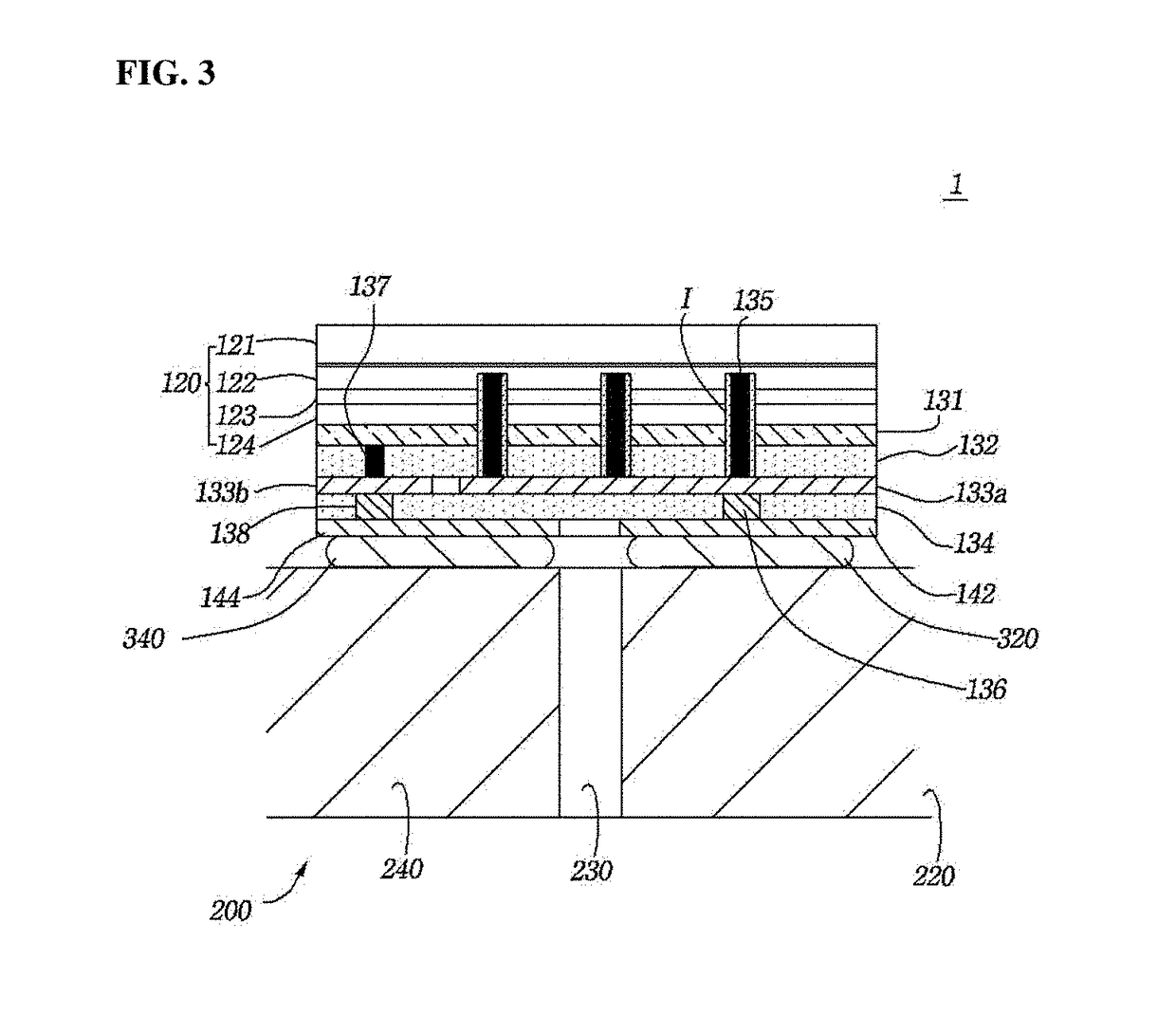
[0027]FIGS. 1 to 3 are perspective, plan, and cross-sectional views of a light emitting element according to one embodiment of the present invention.

[0028]As illustrated in FIGS. 1 to 3, the light emitting element 1 includes an LED chip 100 and a substrate 200 mounted with the LED chip 100.

[0029]The LED chip 100 includes a light emitting semiconductor stack 120 elongated along its major axis and first and second electrode pads 142 and 144 disposed under the light emitting semiconductor stack 120 and spaced apart from each other.

[0030]The first electrode pad 142 and the second electrode pad 144 are elongated along ...


PUM


Abstract

A light emitting element is disclosed. The light emitting element includes: an LED chip including a light emitting semiconductor stack and first and second electrode pads disposed under the light emitting semiconductor stack and spaced apart from each other; a substrate mounted with the LED chip and including a first electrode corresponding to the first electrode pad and a second electrode corresponding to the second electrode pad; a first solder portion connecting the first electrode pad and the first electrode; and a second solder portion connecting the second electrode pad and the second electrode. The first solder portion and the second solder portion are formed without escaping from the mounting area of the LED chip on the substrate by heating a solder material to its melting point or above with an IR laser.

Description

BACKGROUND OF THE INVENTION1. Field of the Invention[0001]The present invention relates to a light emitting element, and more specifically to a light emitting element in which a solder bonding an LED chip to a substrate is prevented from being squeezed out from the mounting area of the LED chip so that the luminous efficiency of the light emitting element is prevented from being lowered by the squeezed-out solder.2. Description of the Related Art[0002]A light emitting element including a substrate and a flip-type LED chip flip-bonded to the substrate is known. The flip-type LED chip of the light emitting element includes a first electrode pad connected to a first conductive semiconductor layer and a second electrode pad connected to a second conductive semiconductor layer. The substrate of the light emitting element includes a first lead electrode electrically connected to the first electrode pad and a second lead electrode electrically connected to the second electrode pad. A solde...

Claims


Application Information

Patent Timeline
Patent Type & Authority Applications(United States)
IPC IPC(8): H01L33/62H01L33/36H01L33/00
CPCH01L33/62H01L33/36H01L33/005H01L33/38H01L2933/0066
Inventor OH, SEUNGHYUNJO, SUNGSIKPARK, JUNGHYUNKIM, BYEONGGEON
Owner LUMENS
Learn More