

Display device
a technology of display device and light source, which is applied in the direction of semiconductor devices, electrical equipment, basic electric elements, etc., can solve the problems and achieve the effects of poor light extraction efficiency and deterioration of light extraction efficiency
- Summary
- Abstract
- Description
- Claims
- Application Information
AI Technical Summary
Benefits of technology
Problems solved by technology
Method used
Image

Examples
Embodiment Construction
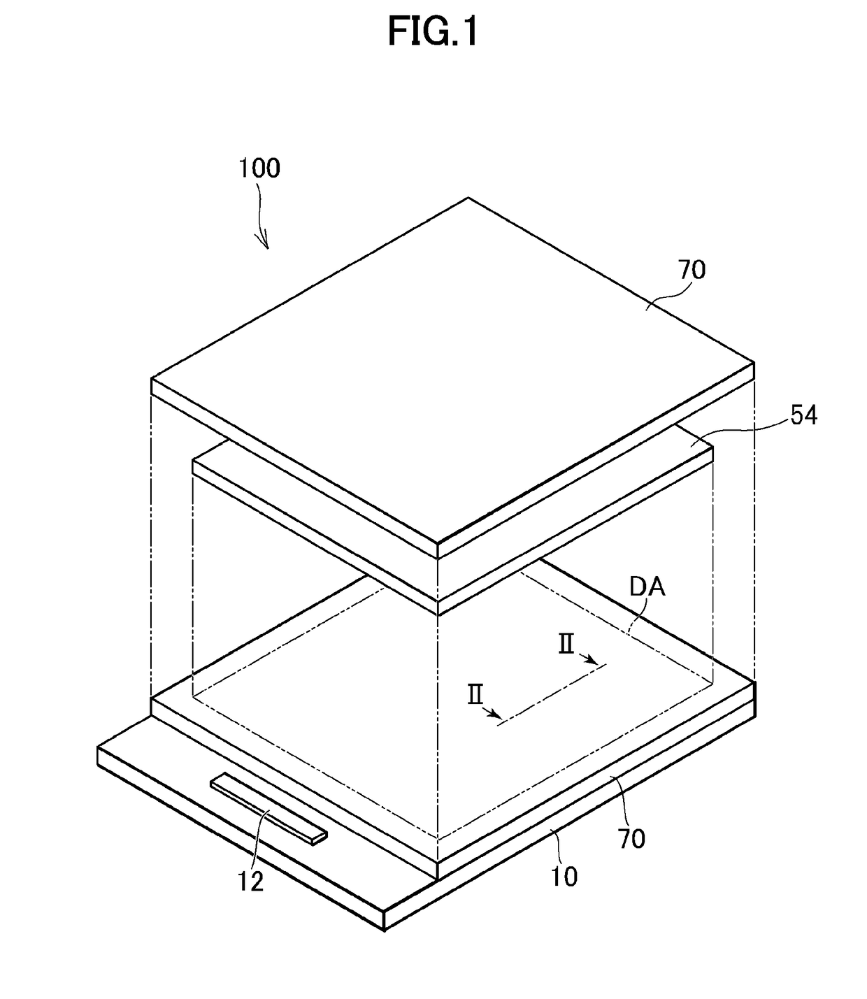
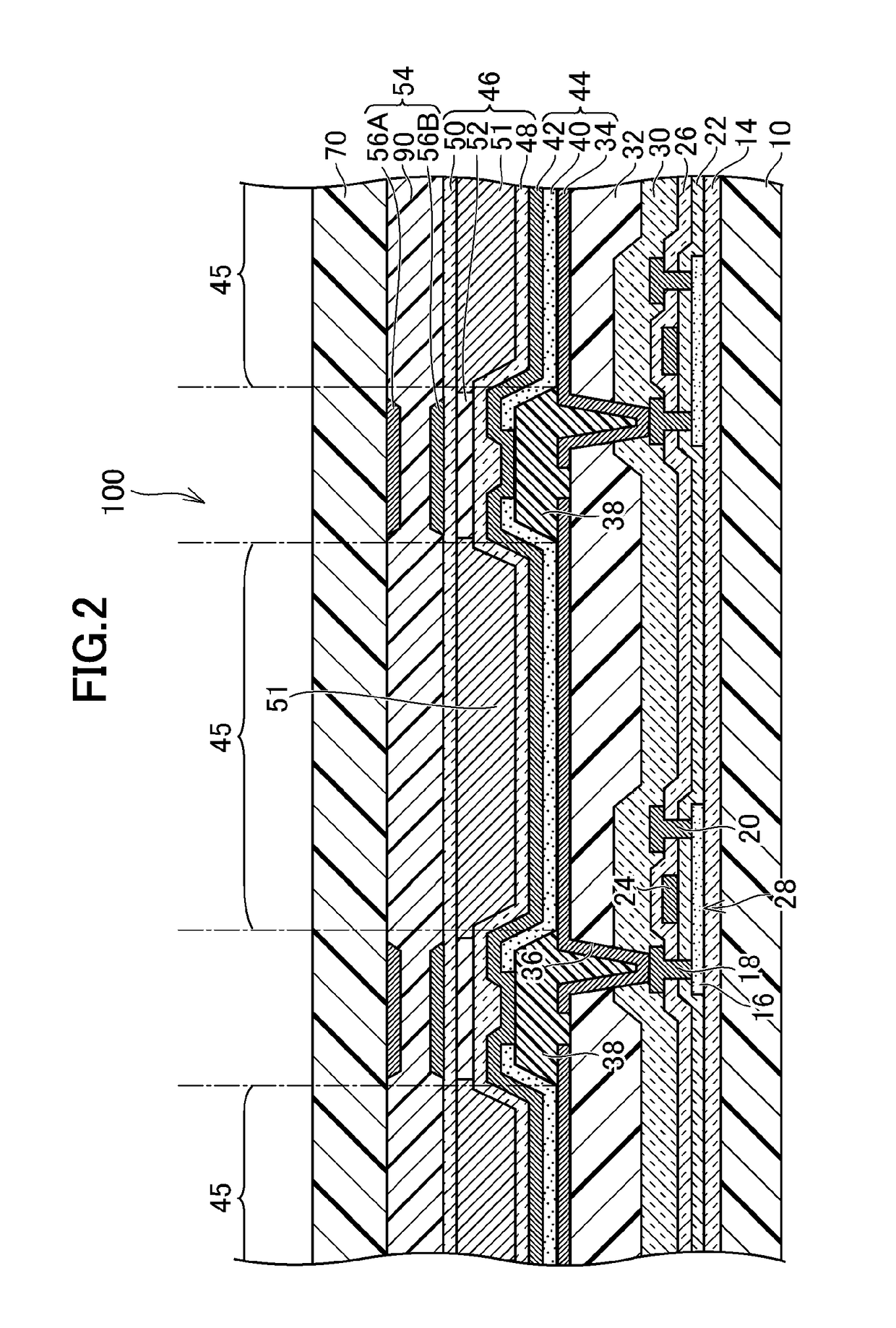
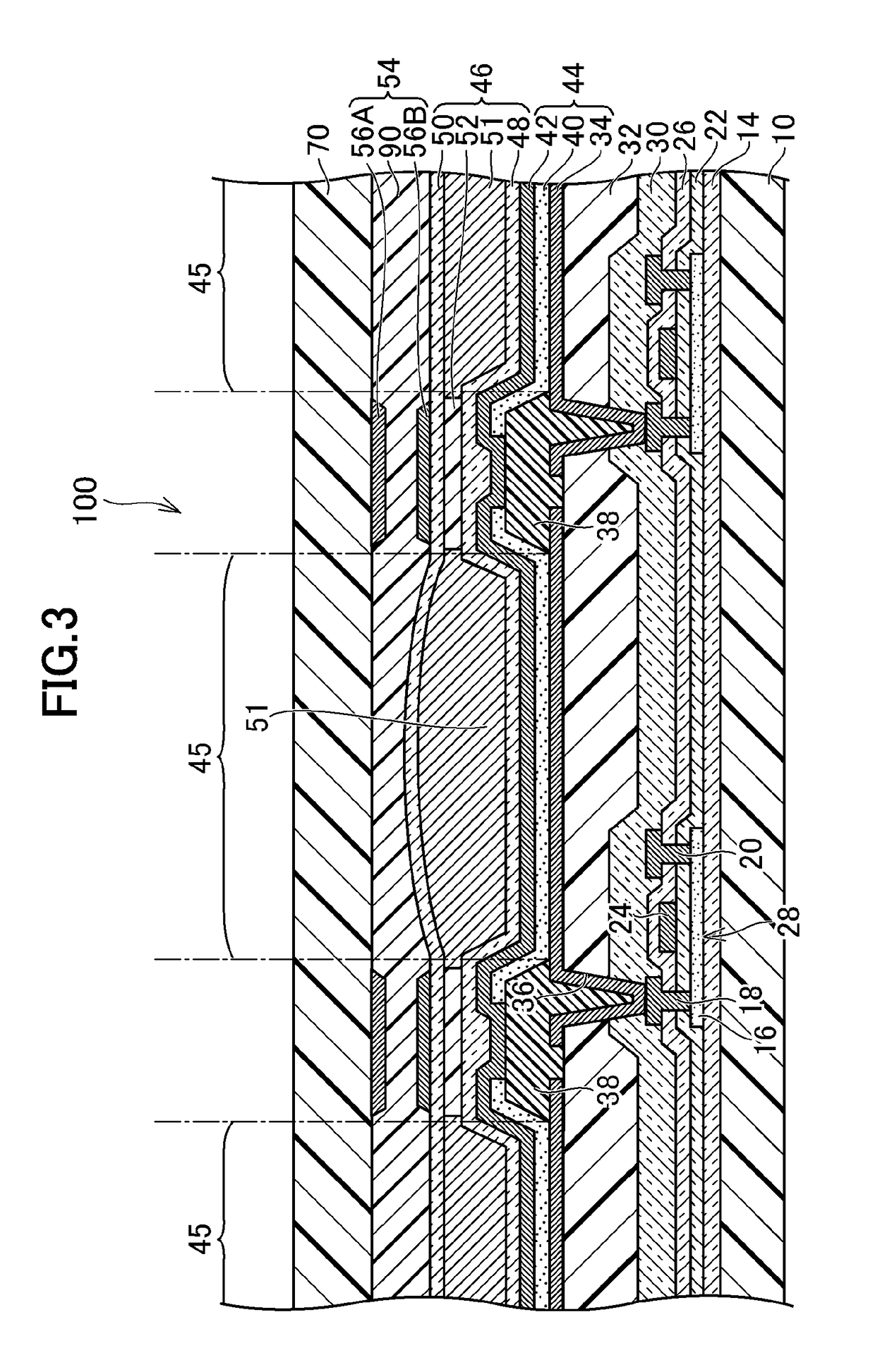
[0025]Hereinafter, the embodiment will be explained with reference to the drawings. Note that the present invention may be achieved in various manners within a scope not departing from the gist thereof and should not be interpreted in a manner limited to the contents of the embodiment to be described below as examples.
[0026]In the drawings, widths, thicknesses, shapes and so on of respective portions may be schematically shown as compared with actual manners for making explanation more clear, and these are just examples and do not intend to limit the interpretation of the present invention. In the specification and respective drawings, the same reference numerals are given to components having functions similar to those explained in the foregoing drawing, and repeated explanation may be omitted.
[0027]Moreover, when the positional relationship between a certain component and another component is defined in the detailed explanation of the present invention, “above”, “on”, “below” and ...
PUM
 Abstract
Description
Claims
Application Information