Self-gating resistive storage device and method for fabrication thereof

a resistive storage and self-gating technology, applied in the direction of electrical equipment, etc., can solve the problems of low fabrication cost of vertical cross array structure, difficult integration of gating tubes, and high lithography step cost, so as to prevent leakage of upper and lower word lines by means of gating layer, the effect of improving the reliability of the devi

Active Publication Date: 2019-03-14
INST OF MICROELECTRONICS CHINESE ACAD OF SCI
View PDF5 Cites 0 Cited by
  • Summary
  • Abstract
  • Description
  • Claims
  • Application Information

AI Technical Summary

Benefits of technology

[0037]The gating layer is grown on the lower electrodes by means of self-alignment technique, such that the interlayer leakage channel running through the gating layer is isolated via the insulating dielectric layers; thus leakage of the upper an

Problems solved by technology

Compared with the multilayer stacked structure, the unit in the vertical direction of the three-dimensional array of the vertical structure is formed by filling a trench once, thus greatly saving an expensive lithography step.
Although the fabrication cost of the vertical cross array structure is low, the problem that gating tubes are difficult to integrate is caused because of the absence of a patterning process for a single device, so it is the k

Method used


Image

  • Self-gating resistive storage device and method for fabrication thereof
  • Self-gating resistive storage device and method for fabrication thereof
  • Self-gating resistive storage device and method for fabrication thereof

Examples


embodiments

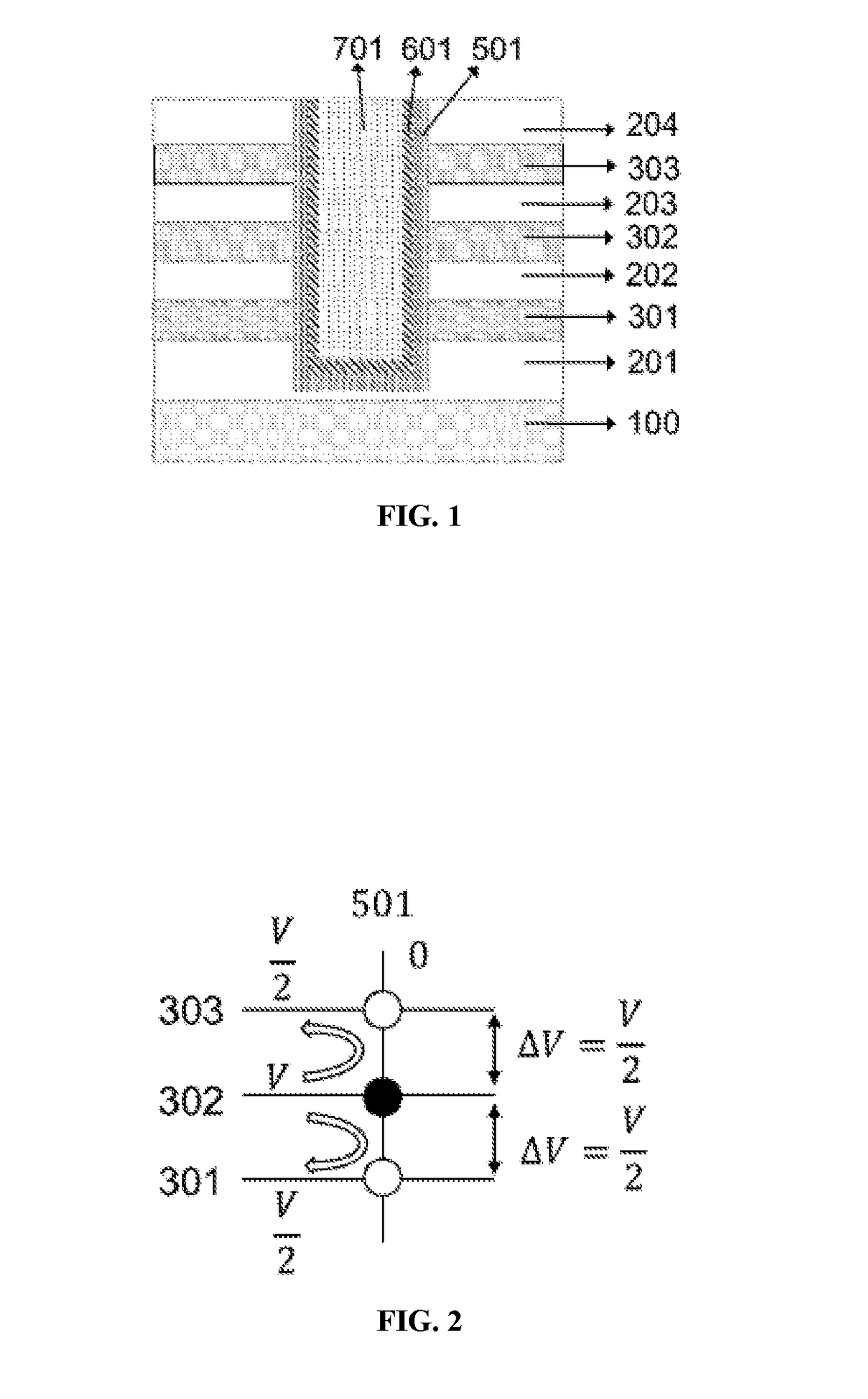
[0049]An embodiment of the present application provides a self-gating resistive storage device, including:

[0050]lower electrodes;

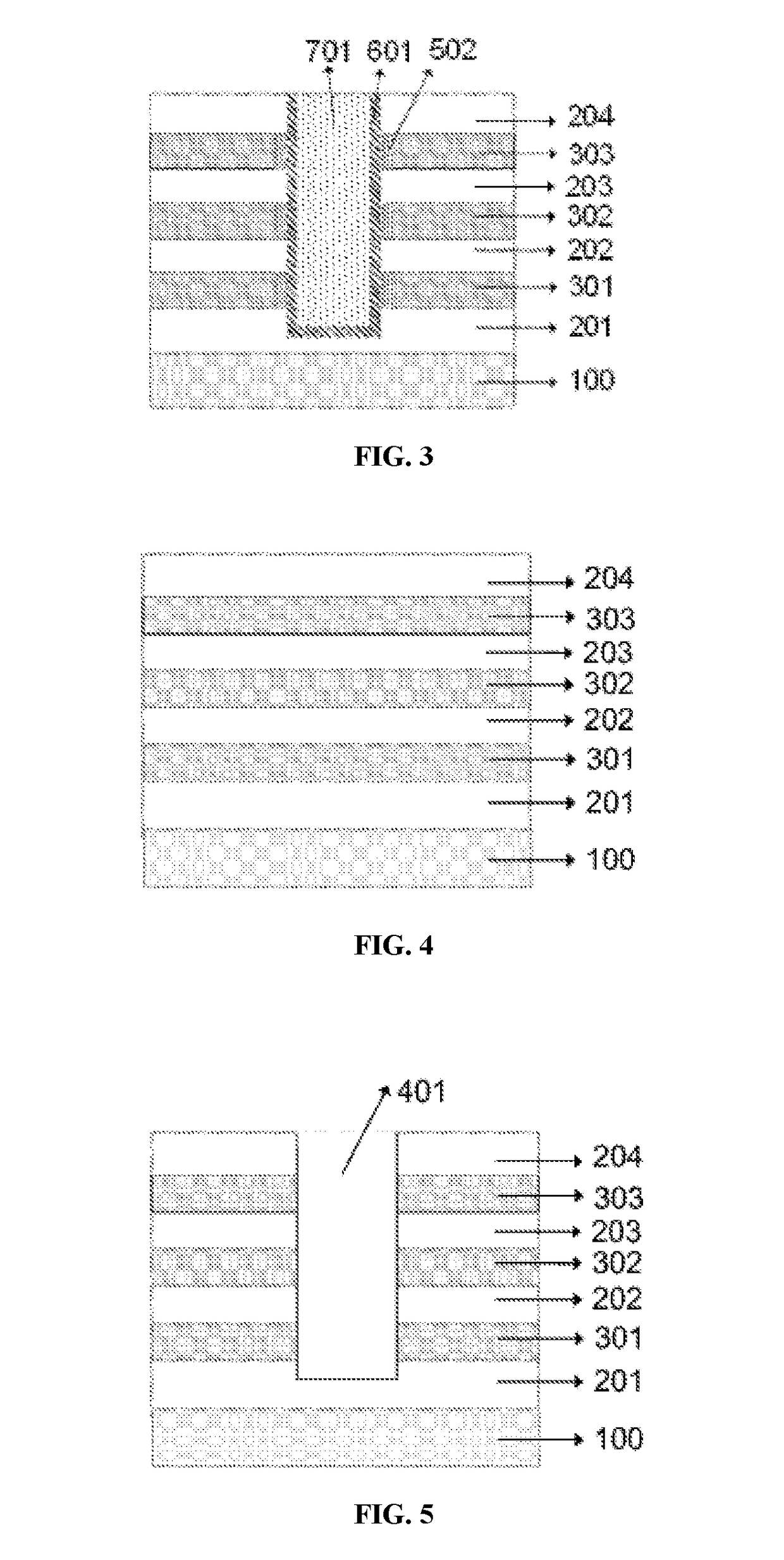
[0051]insulating dielectric layers, arranged perpendicular to, and intersecting with, the lower electrodes to form a stacked structure, said stacked structure being provided with a vertical trench;

[0052]a gating layer grown on the lower electrodes by means of self-alignment technique, the interlayer leakage channel running through the gating layer being isolated via the insulating dielectric layers;

[0053]a resistance transition layer arranged in the vertical trench and connected to the insulating dielectric layers and the gating layer; and

[0054]an upper electrode arranged in the resistance transition layer.

[0055]The self-gating resistive storage device provided by the embodiment of the present application will be illustrated below taking three conductive lower electrodes as an example. However, the present invention does not limit the number of the conduct...


PUM


Abstract

Provided are a self-gating resistive storage device and a method for fabrication thereof; said self-gating resistive storage device comprises: lower electrodes; insulating dielectric layers arranged perpendicular to, and intersecting with, the lower electrodes to form a stacked structure, said stacked structure being provided with a vertical trench; a gating layer grown on the lower electrodes by means of self-alignment technique, the interlayer leakage channel running through the gating layer being isolated via the insulating dielectric layers; a resistance transition layer arranged in the vertical trench and connected to the insulating dielectric layers and the gating layer; and an upper electrode arranged in the resistance transition layer. In the storage device provided by the described technical solution, the gating layer is grown on the lower electrodes by means of self-alignment technique, such that the interlayer leakage channel running through the gating layer is isolated via the insulating dielectric layers; thus leakage between the upper and lower word lines through the gating layer is prevented, solving the technical problem in the prior art of leakage between the upper and lower word lines in a self-gating resistive storage device, and improving the reliability of the device.

Description

TECHNICAL FIELD[0001]The present invention relates to the field of microelectronic technology, and particularly, relates to a self-gating resistive storage device and method for fabrication thereof.BACKGROUND OF THE INVENTION[0002]A resistive memory is of a metal / oxide / metal (MIM) capacitor structure. Under the action of electrical signals, the device is reversibly converted between a high resistance state (HRS) and a low resistance state (LRS) to realize a data storage function. The resistive memory has attracted great attention at home and abroad due to its excellent characteristics in terms of cell area, three-dimensional integration, low power consumption, high erasing speed, multi-value storage and the like.[0003]There are mainly two three-dimensional integration methods for the resistive memory: one method adopts a cross array multilayer stacked structure, that is, a two-dimensional cross array structure is repeatedly fabricated and stacked in multiple layers; and the other me...

Claims


Application Information

Patent Timeline
IPC IPC(8): H01L45/00
CPCH01L45/1233H01L45/1253H01L45/14H01L45/1608H01L45/1675H10B63/845H10N70/823H10N70/20H10N70/8833H10B63/80H10B63/84H10N70/826H10N70/021H10N70/063H10N70/841H10N70/881H10N70/8822H10N70/8825
Inventor LV, HANGBINGLIU, MINGXU, XIAOXINLUO, QINGLIU, QILONG, SHIBING
Owner INST OF MICROELECTRONICS CHINESE ACAD OF SCI
Why Eureka
Try Eureka