Method of manufacturing a split-gate flash memory cell with erase gate
- Summary
- Abstract
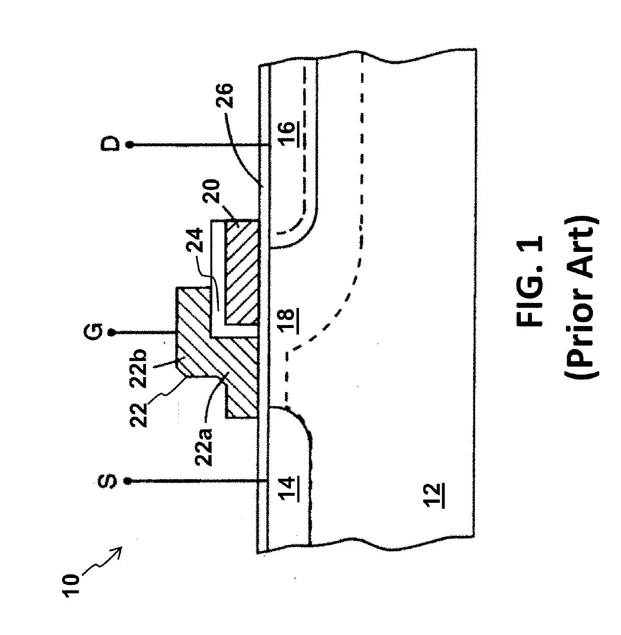
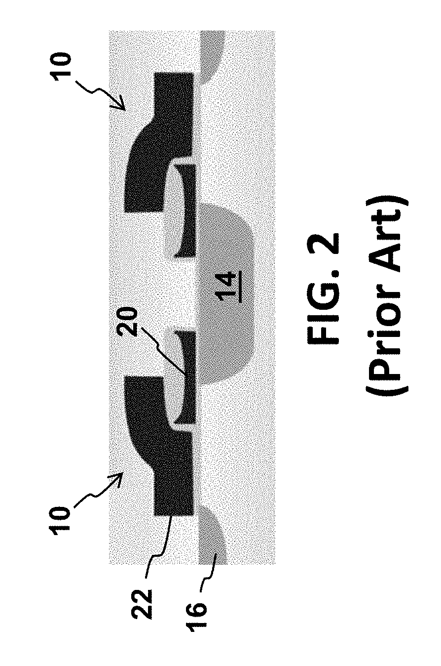
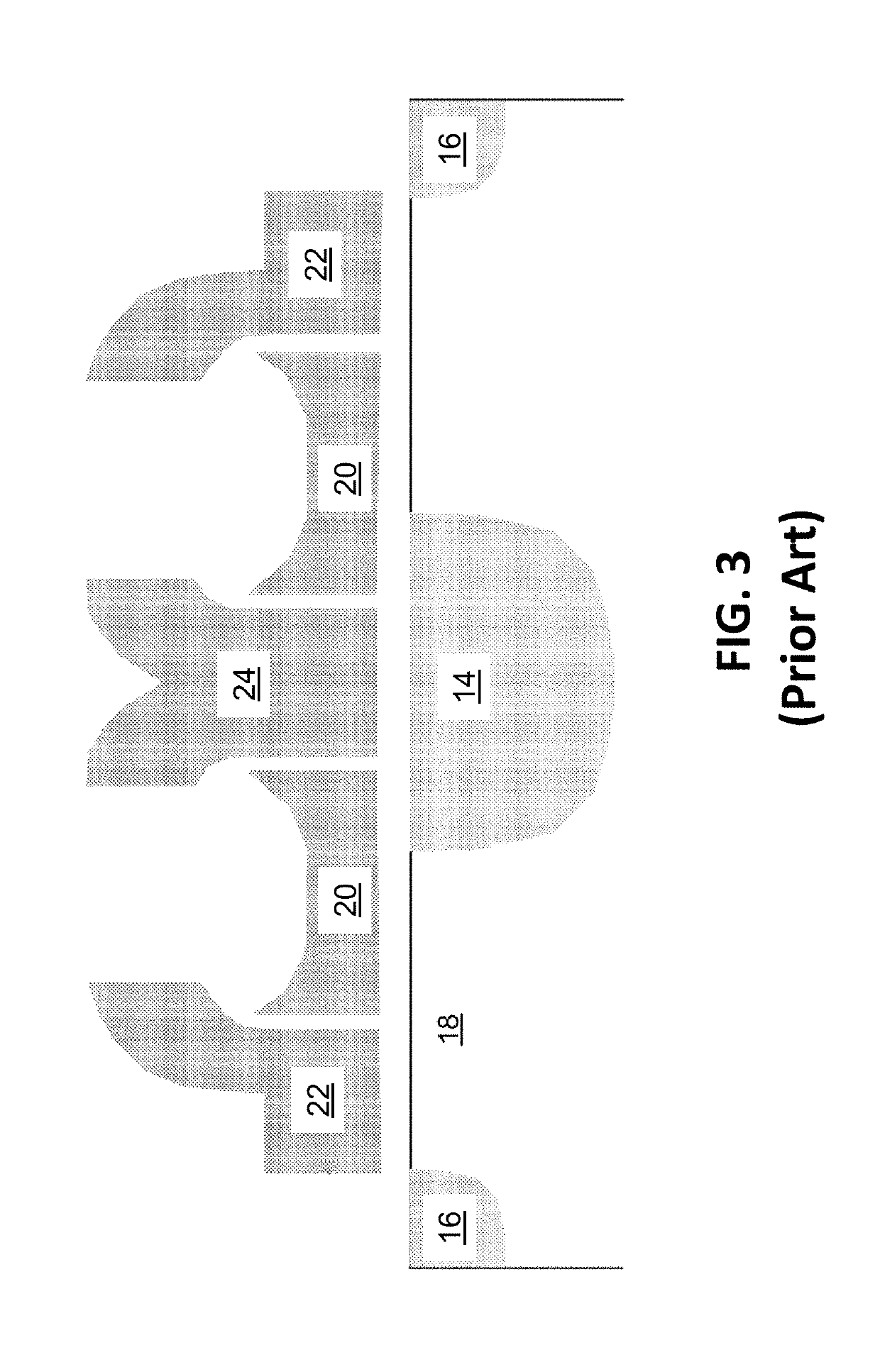
- Description
- Claims
- Application Information
AI Technical Summary
Benefits of technology
Problems solved by technology
Method used
Image

Examples
Embodiment Construction
[0035]The present invention involves a new technique for making three gate memory cells on a substrate on which logic devices are also formed. FIGS. 5A-29A show the formation of the memory cells in the memory area of the substrate, and FIGS. 5B-29B show the formation of low (e.g., 1.2V) and high (HV) logic circuits in a peripheral region of the same substrate, namely a low voltage logic circuit (peripheral) area (LV area) and a high voltage logic circuit (peripheral) area (HV area). The process begins by forming a (pad) silicon dioxide (oxide) layer 42 on the semiconductor substrate 40, followed by a silicon nitride (nitride) layer 44 on the pad oxide layer 42, as shown in FIGS. 5A-5B. A masking step (i.e., photolithography photo resist deposition, exposure, selective photo resist removal) and etch are performed to form trenches 46 extending into the substrate. Trenches 46 separate the LV and HV areas, and separate columns of active regions in which the memory cells are formed in th...
PUM
 Abstract
Description
Claims
Application Information
 - Generate Ideas
- Intellectual Property
- Life Sciences
- Materials
- Tech Scout
- Unparalleled Data Quality
- Higher Quality Content
- 60% Fewer Hallucinations
Browse by: Latest US Patents, China's latest patents, Technical Efficacy Thesaurus, Application Domain, Technology Topic, Popular Technical Reports.
© 2025 PatSnap. All rights reserved.Legal|Privacy policy|Modern Slavery Act Transparency Statement|Sitemap|About US| Contact US: help@patsnap.com