Semiconductor device including error correction code unit, and methods of operating the same

Active Publication Date: 2019-04-04
SK HYNIX INC
View PDF0 Cites 2 Cited by
  • Summary
  • Abstract
  • Description
  • Claims
  • Application Information

AI Technical Summary

Benefits of technology

The present patent is about a semiconductor device that includes an error correction code (ECC) unit capable of easily correcting an error pattern. The device has a controller that receives a request from an external apparatus and generates a data block matrix with a plurality of data block groups and a plurality of parity blocks based on the received data. The encoded data is transmitted to a memory device for storage. The semiconductor device also includes an ECC unit that can detect and correct errors in the data. The technical effect of this patent is to provide a reliable and efficient error correction mechanism for semiconductor devices.

Problems solved by technology

In particular, the concatenated BCH code affects the error floor when a particular error pattern stored in the semiconductor device cannot be corrected.
Such an error pattern may be confined to the message block having the error, but it is difficult to determine a bit of the message block at which the error has occurred, i.e., an error bit.
Accordingly, it is difficult to specifically target the error bit that needs to be corrected.
However, this technique may cause memory cells in the corresponding memory region to deteriorate over time and shorten its lifetime due to multiple read and verify operations.

Method used


Image

  • Semiconductor device including error correction code unit, and methods of operating the same
  • Semiconductor device including error correction code unit, and methods of operating the same
  • Semiconductor device including error correction code unit, and methods of operating the same

Examples


Embodiment Construction

”.

BRIEF DESCRIPTION OF THE DRAWINGS

[0012]The above and other aspects, features and advantages of the subject matter of the present disclosure will be more clearly understood from the following detailed description taken in conjunction with the accompanying drawings, in which:

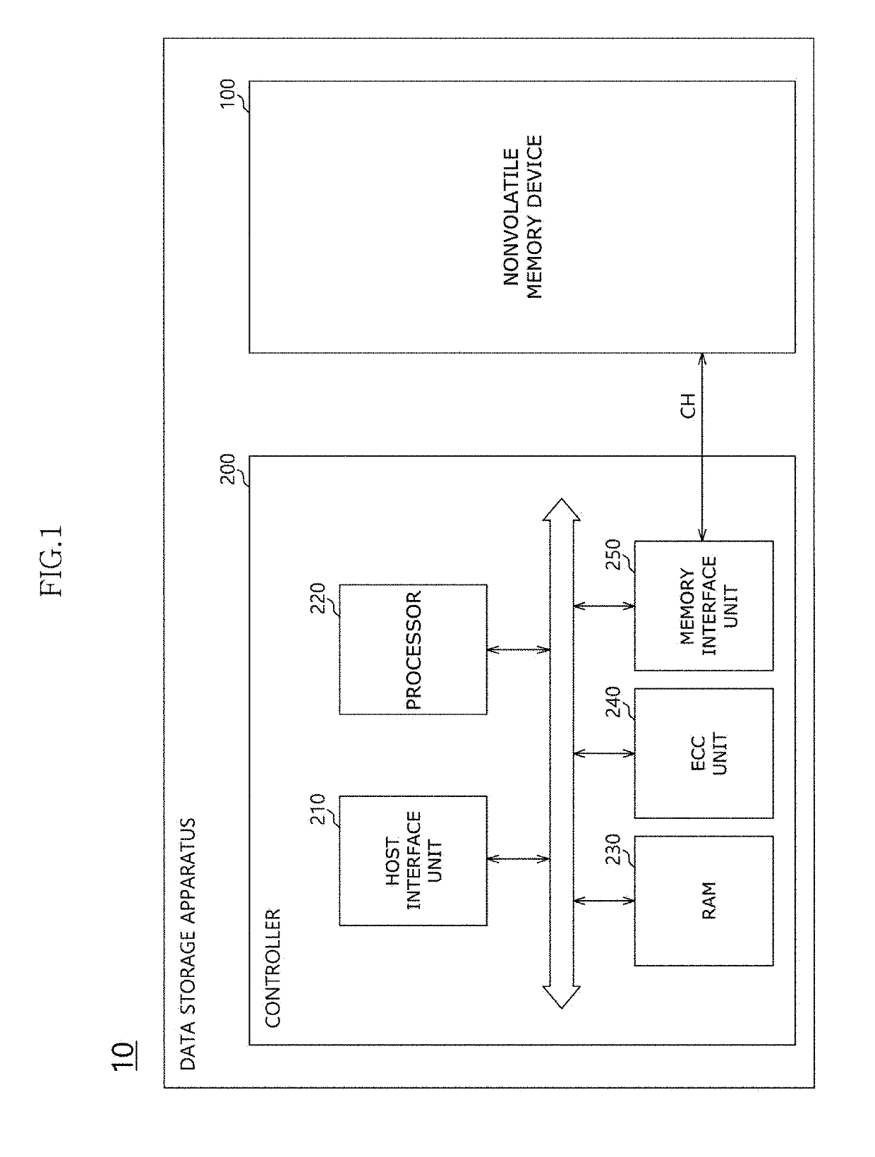
[0013]FIG. 1 is a block diagram illustrating a data storage apparatus according to an embodiment of the present disclosure;

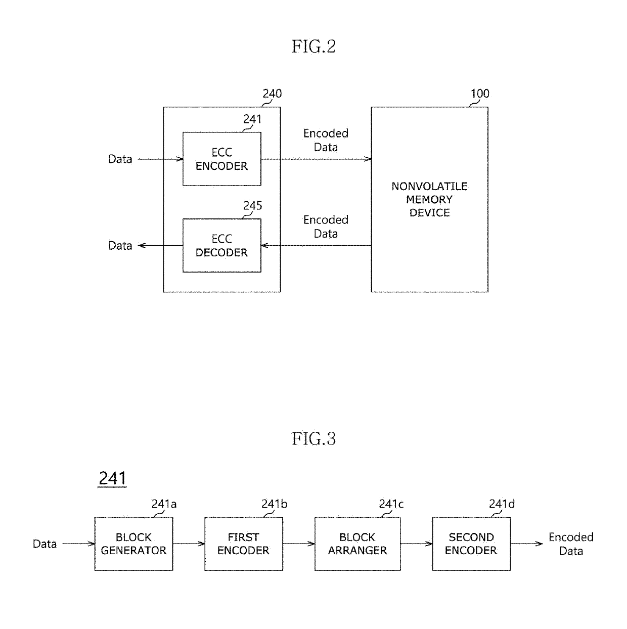
[0014]FIG. 2 is a block diagram illustrating an ECC unit of FIG. 1 according to an embodiment of the present disclosure;

[0015]FIG. 3 is a block diagram illustrating an ECC encoder of FIG. 2 according to an embodiment of the present disclosure;

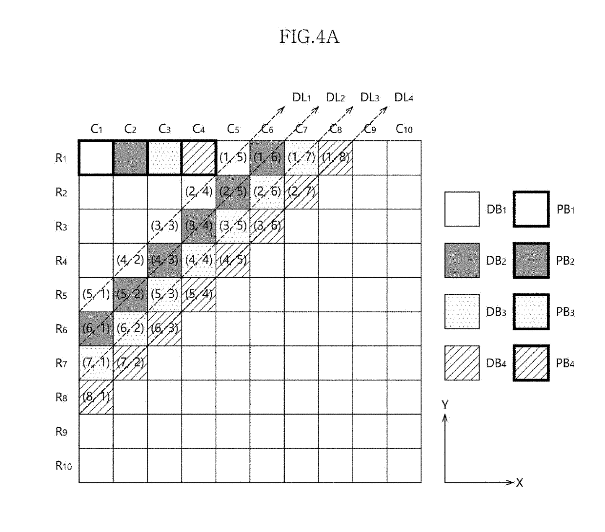
[0016]FIG. 4A illustrates an arrangement of data blocks and parity blocks according to an embodiment of the present disclosure;

[0017]FIG. 4B illustrates a data block matrix according to an embodiment of the present disclosure;

[0018]FIG. 4C illustrates data blocks and parity blocks that are arranged in a three-dimensional (3D) manner according to an embo...


PUM


Abstract

A semiconductor device includes a controller and a memory device. The controller includes a processor configured to process a request from an external apparatus, an interface configured to receive the request and data from the external apparatus and an ECC encoder configured to generate, in response to the request, a data block matrix including a plurality of data block groups and a plurality of parity blocks that are generated based on the received data, and to generate encoded data by adding parity information to the data block matrix, the encoded data being transmitted to the memory device.

Description

CROSS-REFERENCES TO RELATED APPLICATION[0001]The present application claims priority under 35 U.S.C. § 119(a) to Korean patent application number 10-2017-0128487, filed on Oct. 2, 2017, in the Korean Intellectual Property Office, which is incorporated herein by reference in its entirety.BACKGROUND1. Technical Field[0002]Various embodiments of the present disclosure may relate to a semiconductor device, and more particularly, to a semiconductor device including an error correction code (ECC) unit, and an operation method thereof.2. Related Art[0003]Various block-based concatenated encoding and decoding technologies have been used to detect and correct errors occurring in a semiconductor device. A concatenated Bose-Chaudhuri-Hocquenghem (BCH) code technology is a representative example of a block-based concatenated encoding and decoding technology.[0004]In general, in a semiconductor device storing a plurality of message blocks, which employs a coding technology using a matrix of mess...

Claims


Application Information

Patent Timeline
IPC IPC(8): H03M13/29H03M13/09
CPCH03M13/2915H03M13/098H03M13/1515H03M13/152H03M13/2721H03M13/2906H03M13/2909H03M13/2918G06F11/1032
Inventor KIM, DAE SUNGCHAE, CHOL SU
Owner SK HYNIX INC
Why Eureka
Try Eureka