Semiconductor device

Active Publication Date: 2019-04-11
FUJI ELECTRIC CO LTD
View PDF1 Cites 19 Cited by
  • Summary
  • Abstract
  • Description
  • Claims
  • Application Information

AI Technical Summary

Benefits of technology

[0015]In the embodiment, the semiconductor device further includes a third semiconductor region of the first conductivity type provided in the first semiconductor layer, the third semiconductor region being in contact with the second semiconductor layer and reaching a deep position closer to the second electrode from the interface of the first

Problems solved by technology

Nonetheless, when a body diode of a trench gate MOSFET is used in place of an e

Method used


Image

  • Semiconductor device
  • Semiconductor device
  • Semiconductor device

Examples


Embodiment Construction

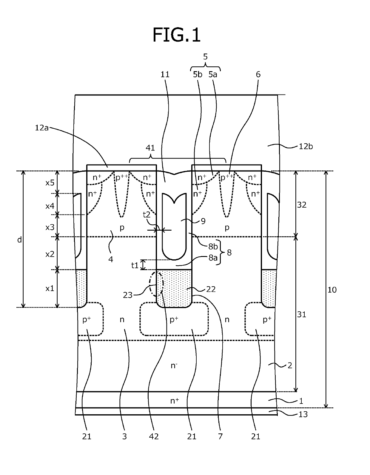
[0031]First, problems associated with the conventional techniques will be described. As described above, in the conventional trench gate MOSFET 131 (refer to FIG. 13) with the trench-type SBD 132 built therein, the trench-type SBD 132 is disposed between the adjacent gate trenches 107. Therefore, the cell pitch (distance between the gate trenches 107) is difficult to reduce and a problem arises in that the ON resistance cannot be decreased.

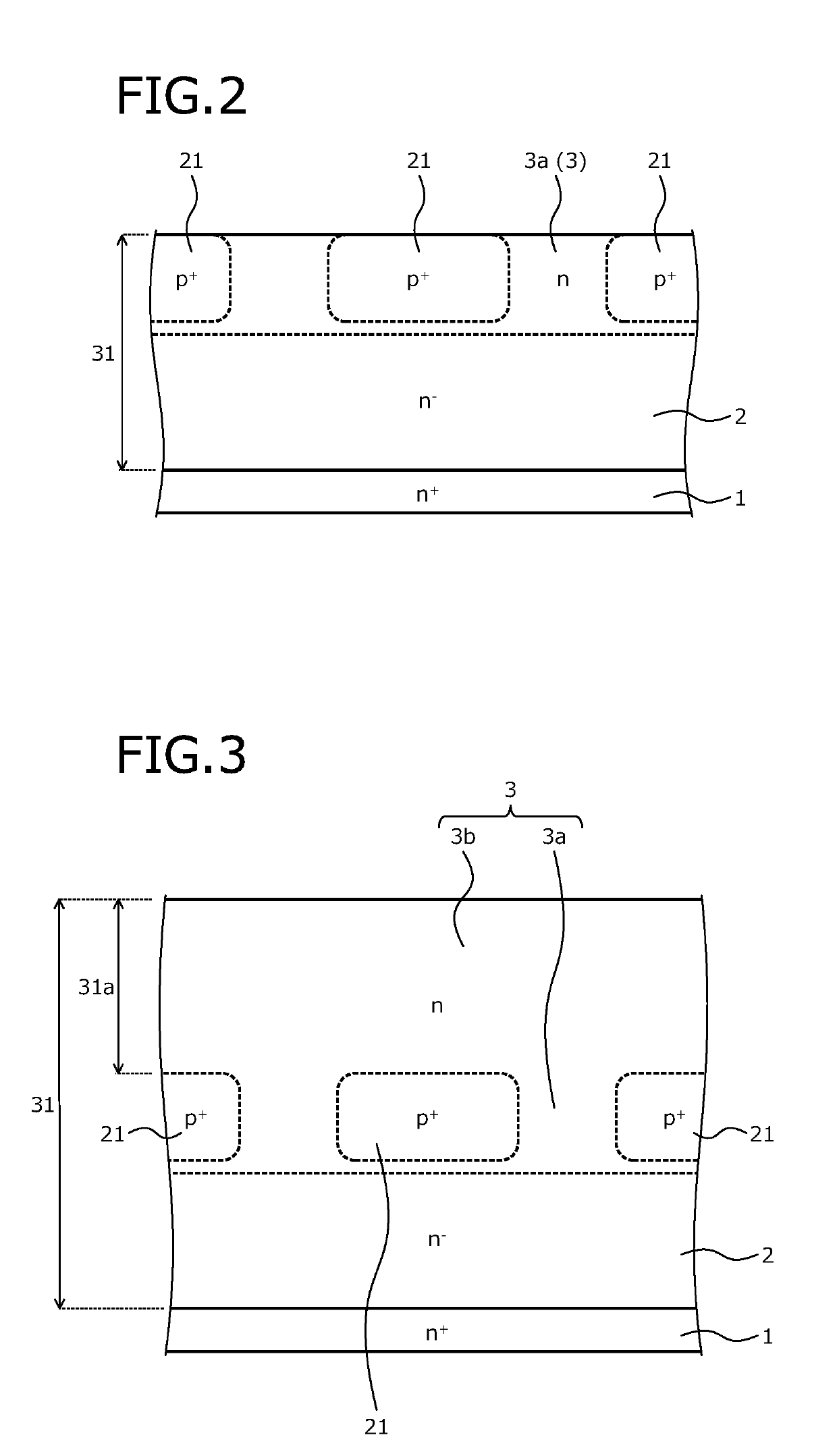
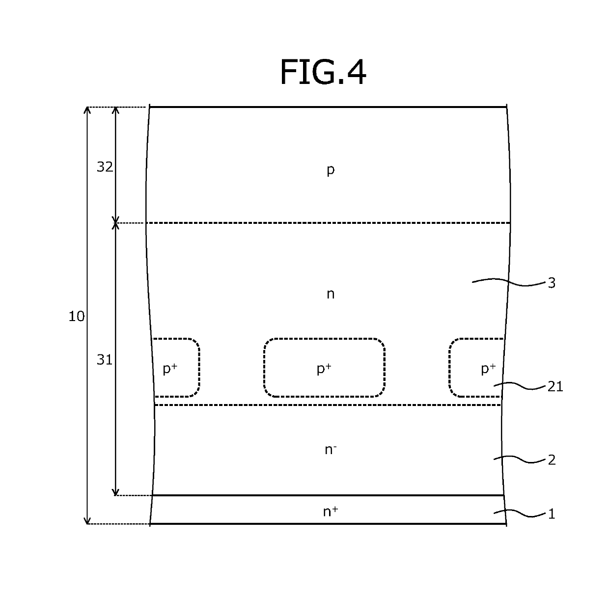
[0032]Embodiments of a semiconductor device according to the present invention will be described in detail with reference to the accompanying drawings. In the present description and accompanying drawings, layers and regions prefixed with n or p mean that majority carriers are electrons or holes. Additionally, + or − appended to n or p means that the impurity concentration is higher or lower, respectively, than layers and regions without + or −. In the description of the embodiments below and the accompanying drawings, main portions that are ident...


PUM


Abstract

At bottom of a gate trench, a conductive layer is provided. A Schottky junction is formed along a side wall of the gate trench by the conductive layer and the n-type current spreading region. The Schottky junction constitutes one unit cell of a trench-type SBD. In the gate trench, a gate electrode is provided on the conductive layer, via an insulating layer. The gate electrode constitutes one unit cell of a trench-gate-type vertical MOSFET. In other words, one unit cell of the trench gate MOSFET and one unit cell of the trench-type SBD are disposed built into a single gate trench and oppose each other in a depth direction.

Description

CROSS REFERENCE TO RELATED APPLICATIONS[0001]This application is based upon and claims the benefit of priority of the prior Japanese Patent Application No. 2017-195480, filed on Oct. 5, 2017, the entire contents of which are incorporated herein by reference.BACKGROUND1. Field[0002]Embodiments of the invention relate to a semiconductor device.2. Description of Related Art[0003]Conventionally, reduced ON resistance is demanded of a power semiconductor device that uses a semiconductor material (hereinafter, wide bandgap semiconductor material) having a bandgap that is wider than that of silicon. For example, in a vertical metal oxide semiconductor field effect transistor (MOSFET), a trench gate structure is adopted that facilitates structurally low ON resistance characteristics as compared to a planar gate structure in which a MOS gate is disposed in a flat plate-like shape on a front surface of a semiconductor chip. A trench gate structure is a MOS gate structure in which a MOS gate i...

Claims


Application Information

Patent Timeline
IPC IPC(8): H01L29/78H01L29/423H01L29/06H01L29/16H01L29/10H01L29/08H01L21/02H01L21/04H01L29/49H01L29/66
CPCH01L29/7806H01L29/4236H01L29/0696H01L29/1608H01L29/1095H01L29/0865H01L21/02378H01L21/02529H01L21/02634H01L21/046H01L21/0475H01L29/0882H01L21/049H01L29/4916H01L29/7813H01L29/0869H01L29/66734H01L29/66068H01L29/7811H01L27/0629H01L29/7827H01L29/0623H01L29/42368H01L29/42376
Inventor KOBAYASHI, YUSUKEHARADA, SHINSUKE
Owner FUJI ELECTRIC CO LTD
Why Eureka
Try Eureka