Silicon carbide wafer and method for production thereof

a silicon carbide wafer and silicon carbide technology, applied in the field of silicon carbide wafers, can solve the problems of leakage phenomena, affecting the quality of epitaxial layers grown from epitaxial films, and serious damage to epitaxial films, so as to improve defects and poor flatness. , the effect of improving the drawbacks

Active Publication Date: 2019-04-18
GLOBALWAFERS CO LTD
View PDF2 Cites 6 Cited by
  • Summary
  • Abstract
  • Description
  • Claims
  • Application Information

AI Technical Summary

Benefits of technology

[0004]The main object of the present disclosure is to effectively improve the drawbacks of defects and poor flatness on the surface of the silicon carbide wafer in the related art.
[0007]As described above, the method for producing the silicon carbide wafer of the present disclosure can efficiently improve the surface flatness of the silicon carbide wafer and reduce scratches or defects (micro-depressions and micro-protrusions) on the surface of the silicon carbide wafer through polishing the first crystal face and the second crystal face of the unpolished surface with the first polishing solution and the second polishing solution, and through the abrasive particles fixed on the polishing pad.
[0008]In addition, the silicon carbide wafer of the present disclosure can provide the scratch-free polished surface and has excellent flatness parameters (Sa is less than 2.5 nm and Sz is less than 20 nm) so as to effectively reduce the defects transmitted to the epitaxial layer and enhance the quality of the epitaxial layer in subsequent applications.

Problems solved by technology

When the surface roughness of the silicon carbide wafer is large, the quality of the epitaxial film will be seriously affected.
Meanwhile, the quality of the epitaxial layer grown from the epitaxial film will also be affected by the surface defects and flatness of the silicon carbide wafer.
These defects not only cause leakage phenomena, but also significantly reduce the electron mobility.

Method used


Image

  • Silicon carbide wafer and method for production thereof
  • Silicon carbide wafer and method for production thereof

Examples


Embodiment Construction

[0013]The aforementioned illustrations and following detailed descriptions are exemplary for the purpose of further explaining the scope of the instant disclosure. Other objectives and advantages related to the instant disclosure will be illustrated in the subsequent descriptions and appended drawings. In addition, for an easy instruction, similar reference numbers or symbols refer to elements alike.

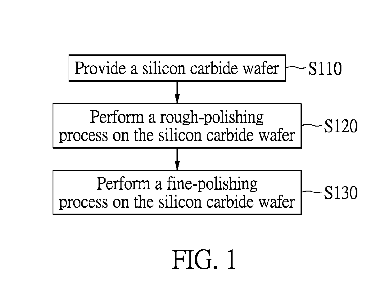
[0014][Method for Producing Silicon Carbide Wafer]

[0015]Referring to FIG. 1, the present embodiment discloses a method for producing a silicon carbide wafer. The method for producing the silicon carbide wafer includes step S110, step S120, and step S130. It should be noted that the order and the practical operation mode of the steps described in the present embodiment can be adjusted as needed, and the present disclosure is not limited thereto.

[0016]Step S110 is to provide a silicon carbide wafer. The silicon carbide wafer has at least one unpolished surface. That is, the silicon carbide...


PUM

PropertyMeasurementUnit
lengthaaaaaaaaaa
heightaaaaaaaaaa
heightaaaaaaaaaa

Abstract

A method for producing a silicon carbide wafer includes: providing a silicon carbide wafer having an unpolished surface; in which the unpolished surface has a first crystal face and a second crystal face; polishing one face of the first crystal face and the second crystal face of the unpolished surface in a first polishing solution by using a polisher; in which the polisher includes a polishing pad and a plurality of abrasive particles fixed on the polishing pad; and polishing the other face of the first crystal face and the second crystal face of the unpolished surface in a second polishing solution by using the polisher; in which a pH value of the first polishing solution is less than or equal to 7, and a pH value of the second polishing solution is greater than or equal to 7. The present disclosure also provides a silicon carbide wafer.

Description

BACKGROUND OF THE INVENTION1. Field of the Invention[0001]The present disclosure relates to a semiconductor wafer and a method for producing the same; in particularly, to a silicon carbide wafer and a method for producing the same.2. Description of Related Art[0002]Silicon carbide wafers, as the wide-bandgap semiconductors, have the features of high thermal conductivity and high saturated electron drift rates. Because of the growing demand for high-speed and high-frequency radio technologies, the wide-bandgap semiconductors are attracting more and more attention. This type of semiconductor devices has many advantages which conventional silicon-based semiconductors cannot have, such as the capability of being operated at higher power levels, higher temperatures, and harsher environments. In fact, metal-semiconductor field-effect transistors (MESFETs) and metal-oxide-semiconductor field-effect transistors (MOSFETs) fabricated on the basis of the silicon carbide wafers have been realiz...

Claims


Application Information

Patent Timeline
Patent Type & Authority Applications(United States)
IPC IPC(8): H01L21/02
CPCH01L21/02024H01L21/02019B24B1/00B24B37/04H01L21/02008
Inventor LIN, CHING-SHANLU, JIAN-HSINLIOU, CHIEN-CHENGLI, I-CHING
Owner GLOBALWAFERS CO LTD
Why Eureka
Try Eureka