Image sensor packaging method, image sensor package and lens module

a technology of image sensor and lens module, which is applied in the field of image sensors, can solve the problems of dimensional limitations and unfavorable further shrinkage of image sensor package, and achieve the effects of facilitating miniaturization, reducing the thickness of the resulting image sensor package, and reducing the cost of production

Active Publication Date: 2019-04-25
INNO PACH TECH PTE LTD
View PDF5 Cites 2 Cited by
  • Summary
  • Abstract
  • Description
  • Claims
  • Application Information

AI Technical Summary

Benefits of technology

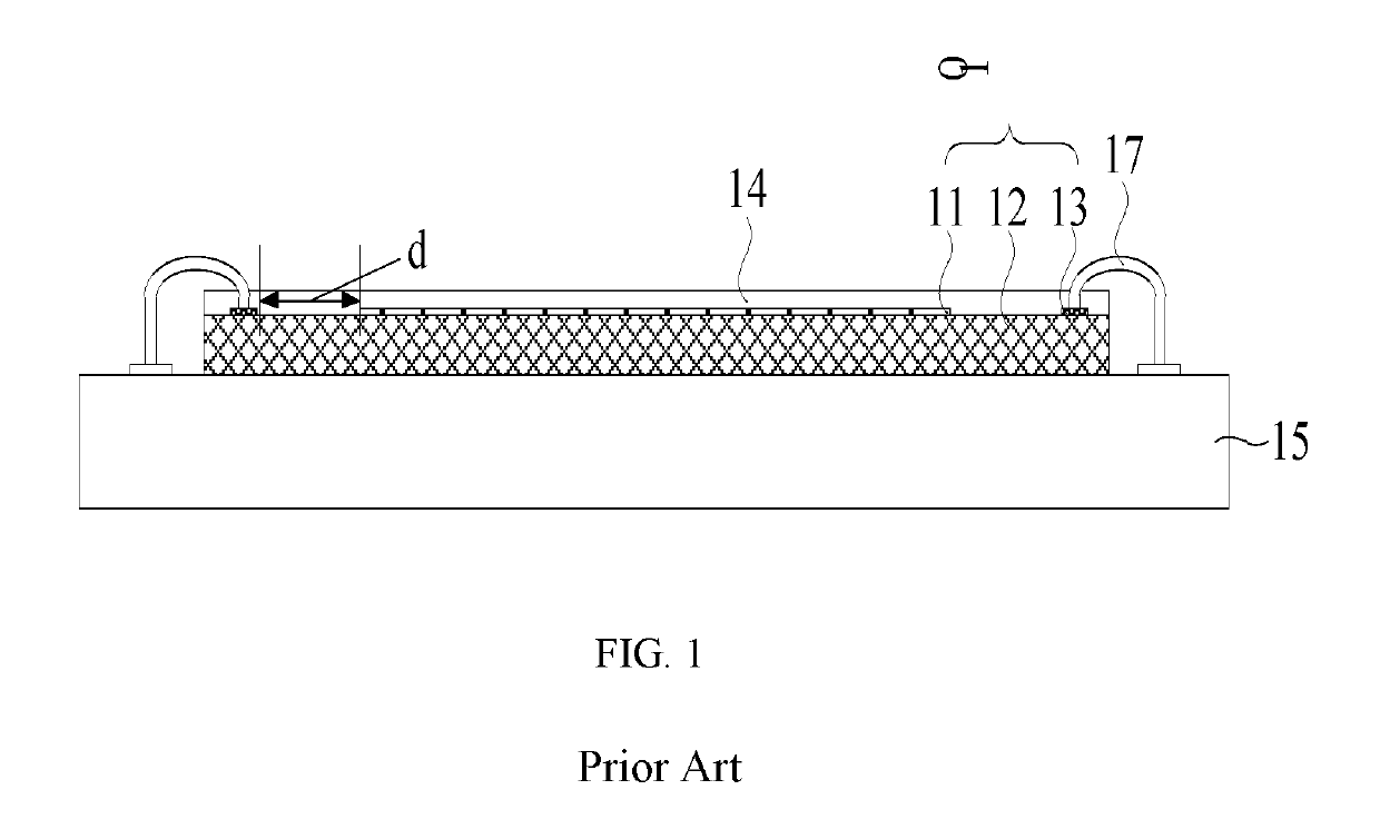
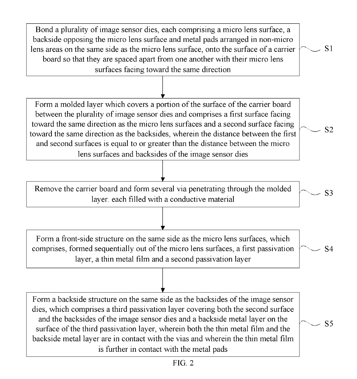
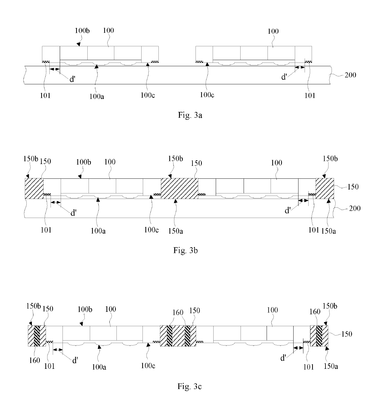
[0031]In the image sensor packaging method according to the present invention, the plurality of image sensor dies are bonded to the surface of the carrier board so that they are spaced apart from one another, and a molded layer is formed between the plurality of image sensor dies, followed by the removal of the carrier board, wherein the thickness of the molded layer is equal to or greater than that of the image sensor dies (the thicknesses of them both refer to their dimensions in the direction perpendicular to the micro lens surfaces). That is, the image sensor dies are embedded in the molded layer. Compared to the conventional COB packaging process, this method allows a smaller thickness of the resulting image sensor package by dispensing with the need for an interconnecting board, which is favor...

Problems solved by technology

This is unfavorable to further shrinkage of the image sensor package.
Moreover, these two disadvantages can...

Method used


Image

  • Image sensor packaging method, image sensor package and lens module
  • Image sensor packaging method, image sensor package and lens module
  • Image sensor packaging method, image sensor package and lens module

Examples


Embodiment Construction

[0038]The image sensor packaging method, image sensor package and lens module proposed in the present invention will be described in greater detail below with reference to specific embodiments which are to be read in conjunction with the accompanying drawings. Features and advantages of the invention will be more readily apparent from the following detailed description and from the figures. However, it is noted that the concept of the present invention can be implemented in various forms and not limited to the specific embodiments disclosed herein. Additionally, the figures are provided in a very simplified form not necessarily presented to scale, with the only intention to facilitate convenience and clarity in explaining the embodiments.

[0039]As used in the specification and claims, the terms “first”, “second” and the like are intended to distinguish similar elements and do not necessarily describe a particular order or time sequence. It is to be appreciated that such terms are use...


PUM


Abstract

An image sensor packaging method, an image sensor package and a lens module are disclosed. In the image sensor packaging method, plural image sensor dies are formed within a molded layer, resulting in a package with a significantly reduced thickness which is favorable to the slimming of the package. The packaging method does not involve any wire bonding process. Instead, metal pads are led out through a thin metal film formed in non-photosensitive areas on the same side of micro lens surfaces of the image sensor dies. This approach has a less adverse impact on micro lens surfaces and, compared to the wire bonding process, allows a smaller spacing from metal pads to the micro lens surfaces with respect to a direction parallel to the micro lens surfaces, which enables more compact image sensor dies usable in a lens module for an optimized spatial design and ease of miniaturization.

Description

CROSS-REFERENCES TO RELATED APPLICATIONS[0001]This application claims the priority of Chinese patent application number 201710986559.X, filed on Oct. 20, 2017, the entire contents of which are incorporated herein by reference.TECHNICAL FIELD[0002]The present invention relates to the field of image sensors and, in particular, to an image sensor packaging method, an image sensor package and a lens module.BACKGROUND[0003]An image sensor is a semiconductor device capable of sensing external light and converting it into an electrical signal. Current integrated circuit (IC) processes allow hundreds or even thousands of image sensor dies to be formed on the same wafer. These image sensor dies are then packaged into image sensor packages, bonded with terminal leads onto their metal pads and provided with lenses and lens holders to form lens modules which can be used in cameras, smart phones, digital cameras, automotive imaging systems, toys and other electronic devices.[0004]A commonly-used...

Claims


Application Information

Patent Timeline
IPC IPC(8): H01L27/146H01L21/56H01L21/768
CPCH01L27/14618H01L27/14627H01L21/568H01L27/14636H01L21/76802H01L21/76877H01L27/14698H01L21/565H01L27/14645H01L27/14623H01L27/14685H01L27/14634H01L27/1469H01L21/561Y02P70/50H01L27/14632H01L2224/24101H01L2224/24155H01L2224/2401H01L2224/24105
Inventor CHANG, LIPINGYU, DEZEZHANG, WANNING
Owner INNO PACH TECH PTE LTD
Why Eureka
Try Eureka